Search This Blog

Powered by Blogger.

Translate

[TC] Remote controlled Spy Bot

Here is a remote operated spy robot circuit which can be controlled by using a wireless remote controller. It can capture audio and video information’s from the surroundings and can be sent to a remote station through RF signals. The maximum range is 125 meters. It overcomes the limited range of infrared remote controllers. This robot consists of mainly two sections. They are explained in detail below.

Remote Control Operated Spy Robot Circuit – Block Diagram
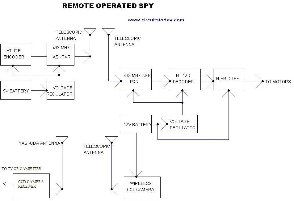
    Remote Control Operated Spy Robot Circuit - Block Diagram
Remote Control Operated Spy Robot Circuit - Block Diagram

1. Remote Control Section

The circuit uses HT 12E, HT 12D encoder and decoder. 433MHz ASK transmitter and receiver is used for the remote control. H-bridge circuits are used for driving motors. Two 12V DC/100RPM gear motors are used as drivers. The working of the circuit is as follows.
When we are pressing any key in remote controller the HT 12E generate 8 bit address and 4 bit data .The DIP switches are used for setting the address. Then the ASK transmitter sends the 8 bit address and 4 bit data to the receiver Then the ASK receiver receives the 8 bit address and 4 bit data and HT 12D decoder decodes the data, thus enabling the appropriate output. Thus the output signals that are generated controls the H-bridge which then rotates the motors.
The 433 MHZ ASK transmitter and receivers are extremely small, and are excellent for applications requiring short-range RF remote controls.  The transmitter module is only 1/3rd the size of a standard postage stamp, and can easily be placed inside a small plastic enclosure. The transmitter output is up to 8mW at 433.92MHz. The transmitter accepts both linear and digital inputs and can operate from 1.5 to 12 Volts-DC, and makes building a miniature hand-held RF transmitter very easy.  The 433 MHZ ASK transmitters is approximately the size of a standard postage stamp
433 MHZ ASK receivers also operate at 433.92MHz, and have a sensitivity of 3uV.  The receiver operates from 4.5 to 5.5 volts-DC.
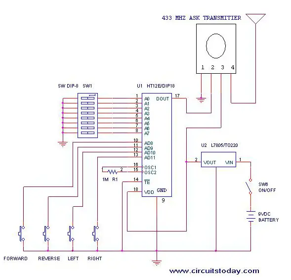
Remote-Control-Operated-Spy-Robot-Circuit-Remote-Control-Section

2. Video Transmission Section

In this project we are using a wireless CCD camera. Now these types of cameras are commonly available in the market. It works on 12VDC supply.


The 12 Volt DC supply is taken from the battery placed in the robot. The camera has a receiver, which is placed in the remote station. Its output signals are in the form of audio and video. These signals are directly connected to a TV receiver or a computer through a tuner card.
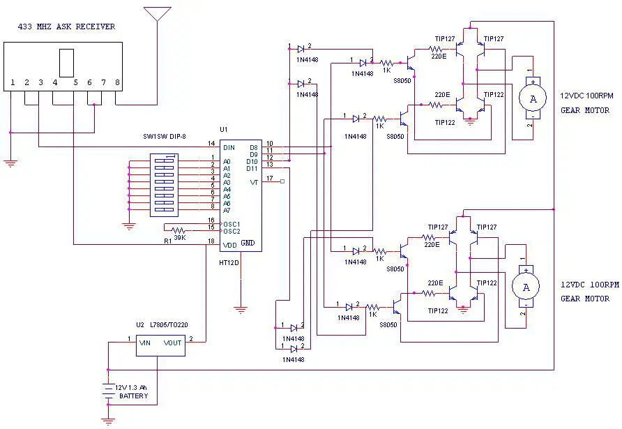
Remote Operated Spy Robot - Remote Control Section

Components Required

IC HT 12E 1
HT 12D 1

LM 7805 2
TRANSISTOR TIP 127 4

TIP 122 4

S 8050 4
DIODE 1N 4148 8
RESISTOR 1K 4

220E 4

39K 1

1M 1
ASK TRANSMITTER 433 MHz 1
ASK RECEIVER 433 MHz 1
DIP SWITCH
2
PUSH TO ON SWITCH
4
GEAR MOTOR 12V DC 100rpm 2
BATTERY 12V 1.3 Ah   rechargeable 1

9V 1
WIRELESS CCD CAMERA
1

Construction

The steps for the construction are…
1. Take a hylam sheet with (20cm*15cm) size.
2. Fix two gear motors (12VDC 100rpm) in the hylam sheet by using aluminum pieces and nut bolts as shown in the figure below.
3. Fix the ball castor as shown in the figure below.
Construction of Remote Operated Spy Robot Circuit
4. Then fix the battery (12VDC 1.2Ah) on the top of the spy robot as shown in the figure below.
Construction of Remote Operated Spy Robot Circuit - Top View
Construction of Remote Operated Spy Robot Circuit – Top View
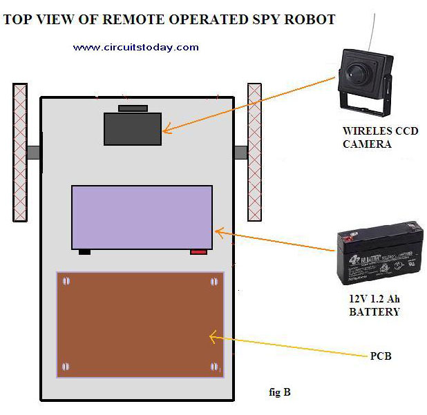
5. Connect two motors to the PCB. The PCB is then connected to the battery.
6. Connect the wireless CCD camera to the battery.
7. Connect the camera receiver to the TV or computer. Video information’s will thus appear in the screen.
8. Switch on the remote controller and control the spy robot


Source: http://www.circuitstoday.com/

[TC] Secure Digital Access System using iButton


Access control forms a vital link in a security chain. Here we describe a secure digital access system using iButton that allows only authorised persons to access a restricted area.


The iButton is used here as a key to the access control system. Its unique identification (ID) number is used for authorisation. On detection of an authorised iButton, the system allows access. Thereafter, an automated lock key locks the system again. The system is permanently halted after five repeated false attempts. A service control unit built around an AVR microcontroller is interfaced to the iButton with 1-wire protocol for authentication of user validation of data.


iButton DS1990A
Here we have used the iButton DS1990A from Dallas Semiconductor (MAXIM). Its block diagram is shown in Fig.1.


Fig.1: Block diagram of iButton
An iButton is a chip housed in a stainless-steel enclosure (refer Fig.2). The electrical interface is reduced to the absolute minimum, i.e., a single data line plus a ground reference. The energy needed for operation is taken from the data line. The DS1990A serial number iButton is a rugged data carrier that acts as an electronic registration number for automatic identification. It contains a unique ROM code that is 64-bit long as shown in Fig.3. The first eight bits are a 1-wire family code. The next 48 bits are a unique serial number. The last eight bits are a cyclic redundancy check (CRC) of the first 56 bits.


Fig.2: A typical iButton chip

Data is transferred serially via the 1-wire protocol, which requires only a single data lead and a
ground return. The iButton DS1990A provides the additional 1-wire protocol capability that allows the search ROM command to be interpreted by the DS1990A.


Fig.3: 64-bit lasered Rom


Circuit description

Fig.4 shows the circuit of the secure digital access system using iButton. The circuit is built around an ATmega16 microcontroller.


Fig.4: Circuit of the secure digital access system using iButton


The ATmega16 is an 8-bit microcontroller based on the AVR enhanced RISC architecture that executes powerful instructions in a single clock cycle. It has 16kB in-system programmable flash program memory with read while- write capabilities, 512 bytes of EEPROM, 1kB SRAM, 32 general purpose input/output (I/O) lines, 32 general-purpose working registers,three flexible timers/counters with compare modes, internal and external interrupts, a serial programmable. USART, a byte-oriented two-wire serial interface, a programmable watchdog timer with internal oscillator, an SPI serial port and six software-selectable power-saving modes.

Piezobuzzer PZ1 is used as an audible indicator for true, fake, random touches and system halt. It is controlled from port pin PD6 of the microcontroller with the help of transistor T1. The iButton socket is connected to port pin PD2. Pull-up resistor R1 is used as required from the 1-wire protocol. Port pin PD4 controls the relay operation through optocoupler PC817 (IC2). The door locking mechanism, say, for a slide door, is connected to the contacts of relay RL1, which closes after some time automatically.

Whenever someone attempts to gain access by touching the iButton (IC5) using his own iButton, the firmware inside the AVR reads its unique ID and matches with the ID in the firmware. If the ID matches, port pin PD4 goes high, the internal LED of the optocoupler (IC2) glows and relay RL1 energises for the predefined time. Simultaneously, the buzzer sounds to indicate grant of access.

Thereafter, relay RL1 de-energises. The buzzer gets the PWM signal to produce sound from port pin PD6 of the microcontroller. The 1-wire communication is done through interrupt port pin PD2 (INT0), so the AVR does not have to poll the pin but respond when any change in signal is detected on the interrupt pin. Switch S1 is used for manual reset.

Port pin PD1 of the microcontroller is used to interface with the hyper terminal of the PC through RS-N 232 interface MAX232 IC (IC3) for iButton verification and checking. The microcontroller  provides a transmit channel for serial data transfer. Transmit data pin (TXD) is specified at port pin PD1. The microcontroller is connected to T1 IN (pin 11) of MAX232. T1 OUT (pin 14) of IC3 is connected to pin 2 of the Comport connector. The signals provided on these pins are TTL-level and must be boosted and inverted through a MAX232 converter to comply with the RS-232 standard.


The MAX232 has two internal charge pumps that convert +5V into ±10V (unloaded) for RS-232 driver operation. The first converter uses capacitor C6 to double the +5V input to +10VM on capacitor C8 at pin 2. The second converter uses capacitor C5 to invert +10V to -10V on capacitor C4 at pin 6.

The power supply for this circuit is derived from 230V, 50Hz AC mains. Transformer X1 steps down 230V, 50Hz AC mains to deliver a secondary output of 9V, 300 mA. The transformer output is rectified by a full-wave rectifier comprising diodes D1 through D4, filtered by capacitor C1 and regulated by IC 7806 (IC4). Capacitor C2 bypasses the ripples present in the regulated supply. LED1 acts as the power indicator and R5 limits the current through LED1.
Construction and testing
An actual-size, single-side PCB for the secure digital access system is shown in Fig. 5(View as PDF) and its component layout in Fig. 6(View as PDF). Assemble the circuit on a PCB as it minimises time and assembly  errors. Carefully assemble the components and double-check for any overlooked error. Connect the assembled circuit to the COM port of the computer. The iButton access code and message is transferred is to the PC through the COM port using the Hyper Terminal program.


Software
The software for this project is given at the end of this article. It is written in ‘Basic’ language and compiled using Bascom-AVR compiler. The source program is well commented and easy to understand.

Burn the finally obtained Intel hex code file into the AVR’s flash memory using a suitable programmer. The microcontroller uses an 8MHz internally generated clock. To activate, program fuse bytes as follows:


Fuse low byte = D4
Fuse high byte = 99

The source program is developed quickly with the help of the BASCOMAVR library function. The 1wrest, 1wread and 1wwrite functions are used for checking the presence of 1-wire device, reading of the unique ID of iButton and writing to the 1-wire device, respectively. Sound function is used for generating the beep sound from the buzzer. The iButton is connected to hardware interrupt pin INT0 so that any change on the pin can be detected and further processing for 1-wire done.
The program execution starts by initialising the input/output ports, the interrupt pin and its level of detection. Global interrupts are enabled and the interrupt service routine is ready to be executed when any interrupt is received. As soon as the normal program execution is interrupted, an interrupt is issued and the control of execution enters the interrupt service routine, where iButton is given reset command first and then the ROM command to fetch the unique ID of the iButton. This fetched ID is compared with the unique ID programmed in the firmware. If there is a mismatch between the two IDs, a fake parameter counter is incremented and the relay connected to port PD4 de-energises. If the two IDs match, the relay connected to port PD4 energises and simultaneously the buzzer connected to port PD6 sounds. If the unique ID is wrong sequentially five times, the system enters the major warning state where the buzzer sounds continuously and it can only be stopped by resetting the system


Author:Chirutkar Harshadkumar Govindrao And Dr. H.N. PandyaSource:http://www.electronicsforu.com/
 

How to build Digital Electronic Lock

Circuit

Digital Electronic Lock

Description

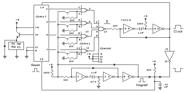
The digital lock shown below uses 4 common logic ICs to allow controlling a relay by entering a 4 digit number on a keypad. The first 4 outputs from the CD4017 decade counter (pins 3,2,4,7) are gated together with 4 digits from a keypad so that as the keys are depressed in the correct order, the counter will advance. As each correct key is pressed, a low level appears at the output of the dual NAND gate producing a high level at the output of the 8 input NAND at pin 13. The momentary high level from pin 13 activates a one shot circuit which applies an approximate 80 millisecond positive going pulse to the clock line (pin 14) of the decade counter which advances it one count on the rising edge. A second monostable, one shot circuit is used to generate an approximate 40 millisecond positive going pulse which is applied to the common point of the keypad so that the appropriate NAND gate will see two logic high levels when the correct key is pressed (one from the counter and the other from the key). The inverted clock pulse (negative going) at pin 12 of the 74C14 and the positive going keypad pulse at pin 6 are gated together using two diodes as an AND gate (shown in lower right corner). The output at the junction of the diodes will be positive in the event a wrong key is pressed and will reset the counter. When a correct key is pressed, outputs will be present from both monostable circuits (clock and keypad) causing the reset line to remain low and allowing the counter to advance. However, since the keypad pulse begins slightly before the clock, a 0.1uF capacitor is connected to the reset line to delay the reset until the inverted clock arrives. The values are not critical and various other timing schemes could be used but the clock signal should be slightly longer than the keypad pulse so that the clock signal can mask out the keypad and avoid resetting the counter in the event the clock pulse ends before the keypad pulse. The fifth output of the counter is on pin 10, so that after four correct key entries have been made, pin 10 will move to a high level and can be used to activate a relay, illuminate an LED, ect. At this point, the lock can be reset simply by pressing any key. The circuit can be extended with additional gates (one more CD4011) to accept up to a 8 digit code. The 4017 counting order is 3 2 4 7 10 1 5 6 9 11 so that the first 8 outputs are connected to the NAND gates and pin 9 would be used to drive the relay or light. The 4 additional NAND gate outputs would connect to the 4 remaining inputs of the CD4068 (pins 9,10,11,12). The circuit will operate from 3 to 12 volts on 4000 series CMOS but only 6 volts or less if 74HC parts are used. The circuit draws very little current (about 165 microamps) so it could be powered for several months on 4 AA batteries assuming only intermittent use of the relay.


XREP – A Combination of Taser and Shotgun

We have already discussed about StunRay Technology and its capability to substitute tasers and guns used in law enforcement. But, there are some limitations to the amount of damage you can do to the suspect if he is not in front of you. That is why tasers are considered more effective as it will leave the suspect electrocuted and numb for a quite a long time, which is more than enough to seize and cuff him up.
But, the tasers used now have a problem of “capability gap”. That is, if the suspect is standing at a distance of 40 feet away from you with a knife, you do have the advantage of using the taser effectively. But if he moves further away with a deadly object in his hand and is ready to use it against you, which will be a problem. The reason is that, most of the tasers work accurately at a range no more than 50 feet. Thus you will be forced to use a gun against the suspect, making the situation more deadly. So, the officers claim that they need a less lethal weapon than a gun and a better weapon than the conventional taser. This is where XREP, comes into action.
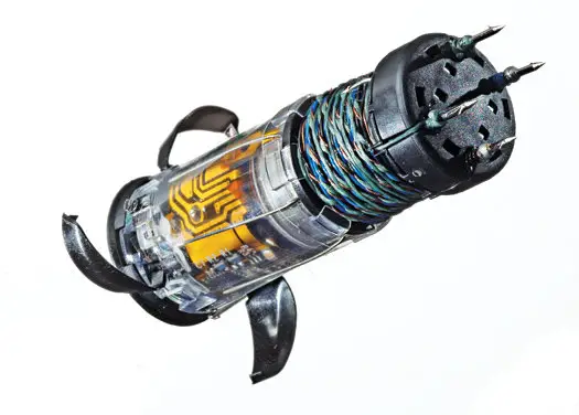
XREP stands for Extended Range Electronic Projectile. It is a twelve gauge wireless projectile that has a firing range of 100 feet and can be capacitated from any kind of pump-action shotgun. As soon as the slug is fired from the gun, it speeds through the air and penetrates the suspect’s skin and causes sudden muscle paralysis. Thus, it is better than a Taser and has the common mechanism of a shotgun.
The manufacturers faced a huge challenge when it came to the design of such a device. One problem they faced was in reducing the overall size of the device. As there is a difference in the amount of voltage that is applied by the device on a human body, the circuit size could easily be reduced accordingly. A conventional taser produces almost 50,000 volts of electricity while a XREP uses no more than 500 volts. While a normal taser arcs the current to the body, this device uses barbed electrodes to pierce the skin. According to the engineer behind the device, Mark Hanchett, the voltage may be very less for a person to be stunned, but it is the waveform produced through it that actually matters. The current produced by the device will cause temporary damage to the nervous system. The developers are trying to upgrade the device by releasing a grenade version that is able to launch up to 200 feet.
Features

Bullet

  • Wireless
  • Size – 12 Gauge
  • Weight – 25 gms
  • Speed – 270 feet/sec
  • Range – 100 feet
  • Current Produced – 1.3 mA
  • Voltage Produced – 500 V
The diagram of a shock bullet taser XREP is shown below.

Shock Bullet TASER XREP
The electrifying bullet can be released from any pump action shot-gun.

Shot-gun Slug

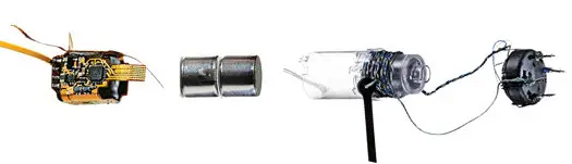
A picture showing the inside of a XREP bullet shell is given below.

XREP Shell
XREP Shell
  • Nose – They are basically 4 electrified barbs that are used to pierce the skin. The shock delivered from the nose will first be sensed around a 6 inch area. This will soon be followed by a bigger shock. The speed and force of impact of nose on the skin will cause the remaining chassis of the device to separate from the nose and dangle downward from a live copper wire.
  • Barbs – If the assailant is not able to get a hold of the wire to complete the circuit, six longer barbs on the projectile can also pierce the skin. The plastic coating of the barbs will be removed as soon as they come in contact with the body and the half-inch electrodes—called “chollas,” pop out like spikes and swing into the body.
  • Hand Trap – The first thought that goes through the assailant’s mind is to grab the dangling wire and rip out the barbs. But, since the wire is pulsing with current, the moment he touches it, electricity will begin to flow from the first set of electrodes in the nose of the projectile to the assailant’s hand. Thus he will be forced to contract from the shock and squeeze the wire tightly. Thus, he will be electrocuted with 15 seconds and will be paralysed.
  • Fins – Just like the fins of a fish, the slug also has three fins attached to its rear end. They are used to help the projectile stay on its track as it sails up to 100 feet toward its target. They will be pressed non, when kept inside the slug. As soon as the slug is fired, they will be opened.
  • Transformer – It is used to produce a small power so as to convert the energy from the battery to discharge 1.3 mA of current for 15 seconds. Morover, it plays an important role in the propogation and interaction of the current to produce the correct waveform.
  • Microprocessor – Once the circuit is complete, an onboard computer commands the voltage capacitor to fire, modulating the intensity, duration and shape of the current.
  • Battery – Two Li batteries are used to provide power for the microprocessor and other circuits.
  • Shell – The circuitry is potted inside shock-absorbing plastic to ensure that it survives the force of the shotgun blast and collision with the target

PIR Sensor Based Security System

The circuit of an inexpensive and highly secure electronic security system is explained below. This electronic security system can be used in banks and other high security areas.
A normal electronic security system will have a transmitter and a receiver. The transmitter sends out an IR laser and this will be received by the receiver. When an intruder walks past the device, the IR beam is cut and thus the alarm is activated. But, this system has some major disadvantages like limited range and poor line of sight. These disadvantages are eliminated through the PIR sensor circuit explained below.

Working

Instead of infrared or laser transmitters and receivers, PIR (Passive Infrared Radial) sensors are used in this circuit. The sensor is basically a pyroelectric device. When the device is exposed to infrared radiation, it generates an electric charge. The device is made of crystalline material. According to the change in the amount of infrared striking the element, there will be a change in the voltages generated, which is measured by an on-board amplifier.
The infrared light explained here refers to the light radiating from all objects in its field of view. The reason for not having a transmitter and receiver is that the device does not emit one, but only accepts the energy emitted from objects above absolute zero in the form of radiations. Thus the temperature will be different for a human working past a sensor, and that of a wall right in front of it. Thus the word “passive” is used in PIR to explain that it does not emit a radiation and receive it, but instead accepts the incoming infrared radiation passively.
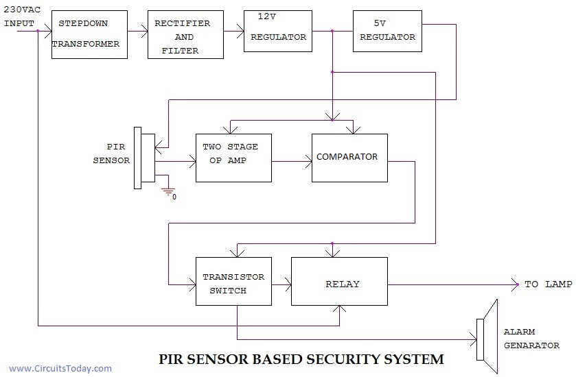
The block diagram of the PIR based security system is given below.
PIR Block Diagram
PIR Block Diagram
The device contains a special filter called a Fresnel lens, which focuses the infrared signals onto the element. As the ambient infrared signals change rapidly, the on-board amplifier trips the output to indicate motion. We can say that the PIR sensor is a human body sensor because it is only activated when a human or animal walks past the sensor. The PIR sensor is the heart of the project. We can design the project in such a manner that as soon as the burglar or intruder walks past the sensor, the alarms would turn on and the whole lighting system could turn on.

Circuit Diagram

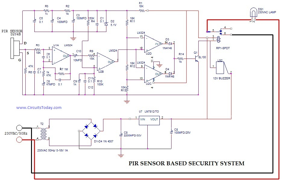
PIR Sensor Based Security System
  • PIR Sensor
D204B PIR sensor is used in this project. The PIR sensor is the heart of the project.
  • Two Stage Amplifiers
Two stage OP-amp: LM 324 is used as two stage amplifier. The signal from the PIR sensor is very low so this signal is amplified by using LM324.LM324 is a quad OP-amp. First two op-amps act as amplifiers.
  • Comparator
The comparator compares the signal from the amplifier and a reference voltage.3rd and 4th OP-amp of LM 324 act as comparator.
  • Transistor Switch
Whenever the output of comparator make HIGH Q1 transistor gets ON and relay will be energized causing the alarm and lamp to turn ON.
  • Power Supply
Power supply converts 230 Volt AC into 12 Volt DC and 5 Volt DC. IC 7812 is used as the 12 Volt voltage regulator and a 5v zener diode act as the 5 Volt voltage regulator

Night security light


Description.
Here is a simple circuit switches on a light around 2 hours after midnight, the time at which most of the robberies taking place.
This simple circuit is build around a CMOS IC 4060 to obtain the required timing. During day time the LDR has low resistance and keeps the pin 12 of the IC1 high, preventing the IC1 from oscillating. When it is dark the LDR resistance becomes high and the pin 12 of IC1 becomes low and the IC starts oscillating, which indicated by the flashing of LED D3.The values of the timing components R1, R2, C4 are so selected that the out put pin3 of IC1 goes high after 8 hours. That means the high output drives the triac to switch on the lamp around 2’O clock. At morning, the LDR resistance drops and the pin 12 of IC1 goes high and stops the oscillation, making the lamp OFF. The switch S1 can be used to manually ON the lamp. The capacitor C2 prevents false triggering.
Circuit diagram with Parts list.
night-security-light
Notes.
  • Assemble the circuit on a good quality PCB or common board.
  • The LDR can be general purpose LDR.
  • The light sensitivity can be adjusted using the preset R6.
  • The IC1 must be mounted on an IC holder

Low cost fire alarm circuit


Description.
When there is a fire breakout in the room the temperature increases.This ultra compact and low cost fire alarm senses fire breakout based on this fact.
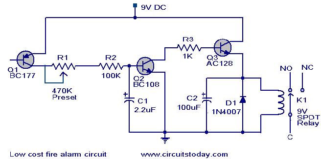
Transistor BC177 (Q1) is used as the fire sensor here.When the temperature increases the leakage current of this transistor also increases.The circuit is designed so that when there is an increase in the leakage current of Q1 ,transistor Q2 will get biased.As a result when there is a fire breakout the transistor Q2 will be on.The emitter of Q2 (BC 108)is connected to the base of Q3(AC 128).So when Q2 is ON Q3 will be also ON.The transistor Q3 drives the relay which is used to drive the load ie,light,bell,horn etc as an indication of the fire.The diode D1 is used as a free wheeling diode to protect it from back EMF generated when relay is switched.
Circuit diagram with Parts list.
fire-alarrm-circuit.JPG
Notes.
  • The Preset R1 can be used to desired temperature level for setting the alarm ON.
  • This is not a latching alarm,ie;when the temperature in the vicinity of the sensor decreases below the set point the alarm stops.
  • The circuit can be powered using  a 9V battery or a 9V battery eliminator.
  • All capacitors are electrolytic and must be rated at least 10V.
  • The load can be connected through the C,NC,NO points of the relay according to your need.
  • The calibration can be done using a soldering iron,and a thermo meter.Switch ON the power supply.Keep the tip of soldering iron near to the Q1.Same time also keep the thermometer close to it.When the temperature reaches your desired value adjust R1 so that relay gets ON.Done

Fire alarm circuit


Description.

Here is a simple fire alarm circuit based on a LDR and lamp pair for sensing the fire.The alarm works by sensing the smoke produced during fire.The circuit produces an audible alarm when the fire breaks out with smoke.
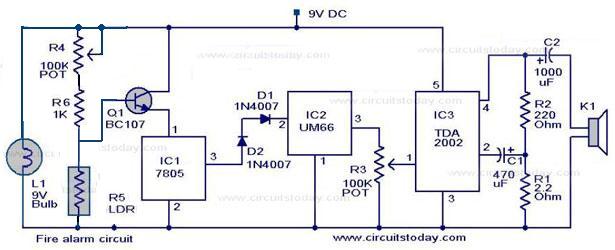
When there is no smoke the light from the bulb will be directly falling on the LDR.The LDR resistance will be low  and so the voltage across it (below .6V).The transistor will be OFF and nothing happens.When there is sufficient smoke to mask the light from falling on LDR, the LDR resistance increases and so do the voltage across it.Now the transistor will switch to ON.This gives power to the IC1 and it outputs 5V.This powers the tone generator IC UM66 (IC2)  to play a music.This music will be amplified by IC3 (TDA 2002) to drive the speaker.Resistor R6 is meant for protecting the transistor when R4 is turned towards low resistance values .Resistor R2 and R1 forms a feedback network for the TDA2002 and C1 couples the feed back signal from the junction of R1 & R2 to the inverting input of the same IC.
The diode D1 and D2 in combination drops 1.4 V to give the rated voltage (3.5V ) to UM66 .UM 66 cannot withstand more than 4V.
Circuit diagram with Parts list.
fire alarm
Fire alarm circuit
Notes.
  • The speaker can be a 32Ω tweeter.
  • POT R4 can be used to adjust the sensitivity of the alarm.
  • POT R3 can be used for varying the volume of the alarm.
  • Any general purpose NPN transistor(like BC548,BC148,2N222) can be used for Q1.
  • The circuit can be powered from a 9V battery or a 9V DC power supply.
  • Instead of bulb you can use a bright LED with a 1K resistor series to it.

Power supply for the circuit.

A well regulated power supply is essential for this circuit because even slight variations in the supply voltage could alter the biasing of the transistor used in the fire sensing section and this could seriously affect the circuit’s performance.
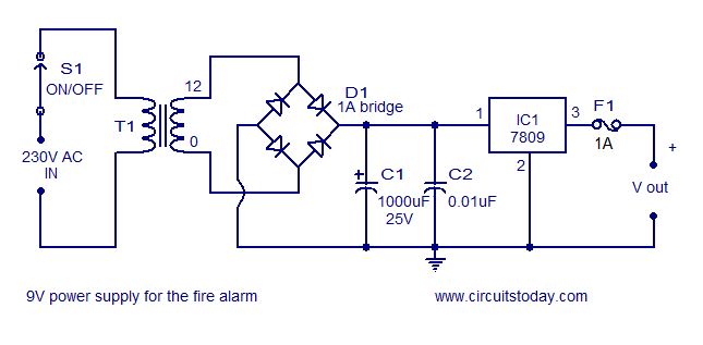
9V power supply
9V/500mA power supply circuit
A regulated 9V/500mA power supply that can be used for powering the basic fire alarm circuit and its modified versions is shown above. Transformer T1 is a 230V primary, 12V secondary, 500mA step down transformer. D1 is a 1A bridge which performs the job of rectification. Capacitor C1 filters the rectifier output and C2 is the AC by-pass capacitor. IC1 (7809) is a 9V fixed positive voltage regulator. The output of the rectifier+filter section is connected to the input of 7805 and a regulated steady 9V is obtained at its output. S1 is the ON/OFF switch. F1 is a 500mA safety fuse.

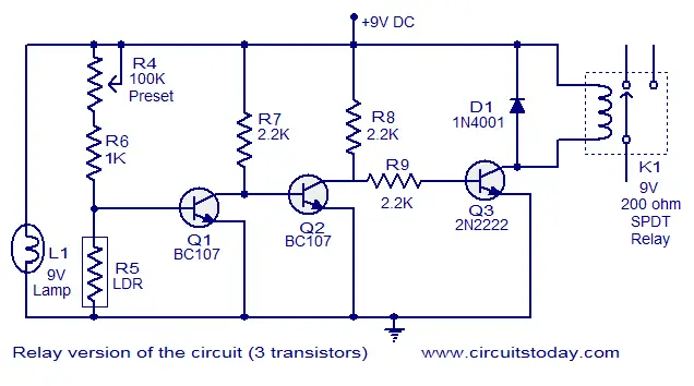
Relay version of the circuit.

Here the above fire alarm circuit is modified to operate a relay when the fire breaks out. The usage of relay makes the circuit able to switch high power warning devices like alarms, bells,beacon lights etc that operates from the mains.
Relay version of the circuit
Two additional transistors are used with the basic fire sensing circuitry (consisting of Q1, R4, R5 and L1) to attain the target. Whenever the fire breaks out the transistor Q1 is switched ON. The collector voltage of Q1 drops to 0.2V and the transistor Q2 gets switched OFF. This makes the collector voltage of Q2 rise towards 9V and this result in the switching ON of transistor Q3. The relay connected at the collector of Q3 is activated and the load connected through the relay contact is driven. Resistors R7 and R8 limits the collector current of Q1 and Q2 respectively. D1 is a freewheeling diode which protects Q3 from the voltage spikes induced when the relay is switched. Resistor R9 controls the base current of transistor Q3 (2N2222)

One transistor code lock


Description.
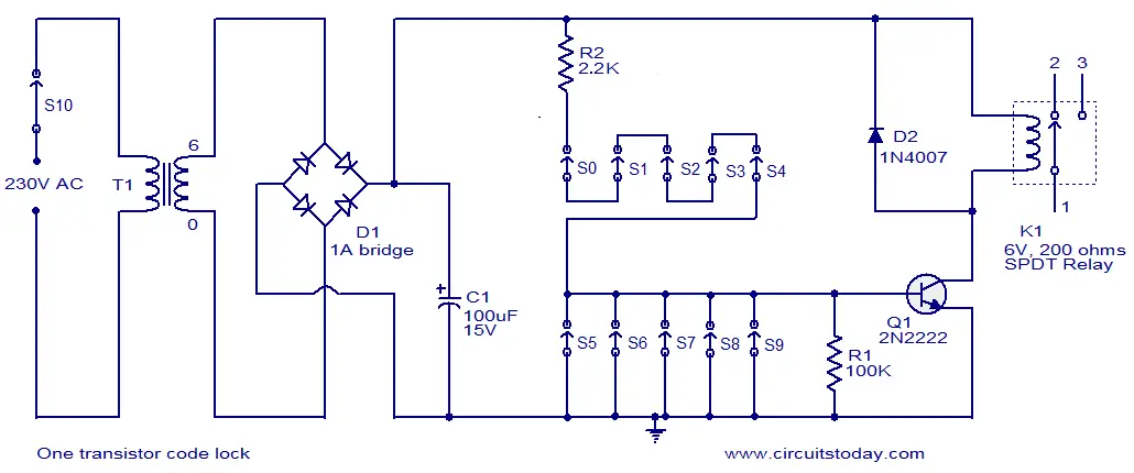
This is of course the simplest electronic code lock circuit one can make. The circuit uses one transistor, a relay and few passive components. The simplicity does not have any influence on the performance and this circuit works really fine.
The circuit is nothing but a simple transistor switch with a relay at its collector as load. Five switches (S0 to S4) arranged in series with the current limiting resistor R2 is connected across the base of the transistor and positive supply rail. Another five switches (S5 to S9) arranged in parallel is connected across the base of the transistor and ground. The transistor Q1 will be ON and relay will be activated only if all the switches S0 to S4 are ON and S5 to S9 are OFF. Arrange these switches in a shuffled manner on the panel and that it. The relay will be ON only if the switches S0 to S9 are either OFF or ON in the correct combination. The device to be controlled using the lock circuit can be connected through the relay terminals. Transformer T1, bridge D1, capacitor C1 forms the power supply section of the circuit. Diode D2 is a freewheeling diode. Resistor R1 ensures that the transistor Q1 is OFF when there is no connection between its base and positive supply rail.
Circuit diagram.
one transistor code lock
Notes.
  • This circuit can be assembled on a Vero board.
  • Switch S1 is the lock’s power switch.
  • The no of switches can be increased to make it hard to guess the combination.
  • Transistor 2N2222 is not very critical here. Any low or medium power NPN transistor will do the job


Shock alarm circuit


Description.
Here is a simple shock sensitive alarm circuit that has many many applications fro home to automobiles.The main application of this circuit is to use it as an anti theft alarm in automobiles.A peizo electric sensor is used as the shock sensor which has to mounted on the door which you have to protect.
Here the IC1  LM 3558 is wired as an inverting Schmitt Trigger.The POT R1 sets the threshold voltage of the circuit.R1 is used as a feed back resistor.When not activated the out put from the piezo sensor will be low and so do the output of the IC.When the piezo sensor is activated its output voltage goes high and triggers the Schmitt trigger.This results the beeping of the buzzer.The buzzer remains beeping for some time even if the vibration is removed.this is because the increase in the inverting input has little effect when the IC is triggered and the state can’t be easily reversed.
Circuit diagram with Parts list .
shock-alarm-circuit.JPG
Notes. 
  • A 3 v battery can be used as  power supply.
  • Fix the sensor firmly to the surface,where ever you place it.
  • It is always good to place the sensor near to the door knob.
  • Adjust R2 to obtain the required sensitivity.
  • Assemble the circuit on a good quality PCB or common board.
  • Use a IC holder for mounting the IC

Page Rank

google pagerank

Write For Us

Submit a Guest Post

Find us on Facebook

Categories

555 Timer IC 7 segment Display 8051 Project AC Circuits Adafruit Alarms Amplifier Circuits Analog Circuits android Arduino arm processor Assembly Languange Atmel Atom Size Audio Circuits augmented reality Automotive Circuits avr Battery Circuits Bicycle Gurad bluetooth Cable TV Circuits Cambridge University Camera Technology Circuit Boards Clipping And Clamping Circuits Clocking And Timer Circuits Computing contact lens Contact Us Form Contests Controller Circuit Conversion Circuits Counter Circuits Digital Electronics diy circuits Downloads EFY EFYTimes Electronic Books Electronic Components Electronic Locks And Keys Engineering Fan Circuits Filter Circuits Fire Alarm free Frequency Fun And Game Circuits future Google Hack n Mod Ham Radio Circuits heart rate monitoring High Voltage Circuits Home Circuits IC Guide ieee Industrial Circuits Infrared Instructables Inventions ipad lcd Led Circuits Light Related Lighting Circuits Medical Circuits Meter Clocks Microcontrollers Microprocessors Mini Projects modules Movie maker NatGeo Navigation Notice Optical Fiber PC Circuits PCB Boards Physics pnp transistor Power Supplies Printing Projects Programmer Project Ideas Projectors Protection circuits Proximity Detectors Radar Radio Circuits Radio Transmitters Raspberry Raspberry Pie Remote Circuits Retis Lab RFID Robot Cars Robotics Science Science Alert Security And Safety Sensor Circuits Servo Motors Smallest Smartwatches sms Software solar cell sound application Spectram Switch Technology News Telephone Related Television Related Test And Measurement Circuits Thermal Projects Tone generator circuits Touch Screen Tutorials Wearables Wi-Fi Wireless
Like us on Facebook
Follow us on Twitter
Recommend us on Google Plus
Subscribe me on RSS