Search This Blog

Powered by Blogger.

Translate

[TC] Simple Rain Alarm

GIVES BEEP WHEN WATER IS IN CONTACT WITH THE WIRE

Rain Alarm Project view

Water is a conductor of electricity. When water is in contact with the probe then there is a flow of current which reaches to the base of Q1. Transistor Q1 is a NPN transistor which conducts. With the conduction of Q1 electron reaches to Q2 which is a PNP transistor .Q2 also conducts and current flows through the speaker. In a speaker there is inductive coil which causes motion in one direction and also produce induce current which is in opposite direction to the flow of current this induce current in the form of pulse flows through a capacitor, resistance and switches off Q1 and relax .this process repeats again and again till probe is in contact with water or we can say there is a oscillation in the circuit thus speaker diaphragm vibrates and gives a tone. Frequency of the circuit depends on the value of Speaker Coil impedance, Capacitor and Resistance Value.

Circuit Diagram of Rain Alarm

[TC] Ultrasonic Proximity Detector

This ultrasonic proximity detector comprising independent, battery-powered transmitter and receiver sections makes use of a pair of matched ultrasonic piezoceramic transducers operating at around 40 kHz each. This circuit can be used in exhibitions to switch on prerecorded audio/video messages automatically when a visitor evincing interest in a product comes near an exhibited product.

Fig. 1: Transmitter circuit
Fig. 1 shows the transmitter circuit. It comprises CMOS timer IC 7555 (IC1) configured as an astable multivibrator, which may be tuned to the frequency of the ultrasonic piezoceramic transmitter’s resonant frequency of around 40 kHz using preset VR1. A complementary pair of transistors T1 and T2 is used for driving and buffering the transducer while it draws spikes of current from IC1 circuit to sustain oscillations and thereby avoids any damage.

The receiver front-end (refer Fig. 2) is designed to provide a very high gain for the reflected faint ultrasonic frequency signals detected by the ultrasonic transducer. The amplifiers built around N1 and N2, respectively, provide AC voltage gain of around 80 each. These two stages should have a high open-circuit gain, wide bandwidth and very low bias current apart from being capable of single-supply operation. Quad op-amp LM324 is used here due to its low cost. For higher efficiency, you may use single op-amps such as CA3130 or CA3140.

Fig. 2: Receiver circuit


Fig. 3: Pinconfigurations oftransistors BC327and BC337
When a visitor pauses before a sistor R10 is used to meet this requirement. The filter also helps to bypass brief bursts of ambient noise in the ultrasonic range. The third stage comprising N3 works as a comparator to provide a triggering pulse when a visitor stops by. This pulse can be used to trigger a timer or a monostable, whose output may then be used to switch on the audio/video message concerning the product for a predetermined period.

When somebody comes in front of the ultrasonic piezoceramic transducer pair, the status LED (LED1) glows because of the signal reflected from the body of the visitor.

The circuit can be assembled on any general-purpose PCB. The transmitter and the receiver should be aligned such that the transmitted ultrasonic signal is optimally received by the receiver after reflection. Fig. 3 shows the pin configuration of transistors T1 and T2, while Fig. 4 shows installation of the ultrasonic piezoceramic transducer pair operating at around 40 kHz.


Source: http://electronicsforu.com/
 

Fig. 4: Installation of transducer pair

[TC] ExpeditInvaders Shelf -Arduino Based LED Lighting Shelf


Currently ExpeditInvaders support 10 color sets (RGB, Rasta, CGA, Brazil, Fizz, Kitty, Neon, Lantern, Lemming, LeBron) and 6 animation modes (Random, Solid, Ordered, Checkboard, Weird, Weirdtwo). The best thing about ExpeditInvaders is, that you can use your feets to change the color set or animation mode. Under the shelf is a PS2 keyboard attached. The keyboard has a special key map installed, if a key on the left side is pressed the color set change, if a key on the right side is pressed the animation will change.
If you press ESC + Arrow Right ExpeditInvaders will save the current state to the EEPROM. This state will be restored next time ExpeditInvaders is restarted.

All you need to spice up your Expedit Shelf are two strands of LED modules, an Arduino board (doesn’t matter which one, can be an old Duemilanove or a new Leonardo) and an old PS2 Keyboard.

Step 1, align LED Modules
Align the modules like on this image (back view):

It should look like this, once you installed them:


Step 2: Connect Devices to Arduino
Connect Pin 13 to LED Module Clock, Pin 11 to LED Module Data and GND to LED Module GND.
Connect 5v and GND to the PS2 Module, Connect Data to Pin 2 and Clock to Pin 3.

You can use an Arduino without pinheaders (solder direct on the board) or you use a ProtoShield Kit.

Here is the PS2 connection schema (thanks to prjc.com, I ripped your image):


Step 3: (Hot) Glue keyboard under the shelf
Just hot glue the keyboard under the shelf, make sure the cable is correct aligned. Now you can kick your Arduino Project…


Step 4: Upload Firmware to Arduino
Get the ExpeditInvaders Firmware on my GitHub repo and upload it to your Arduino board.


Step 5: Connect 12V to the Arduino and LED Modules
Connect 12V to the Arduino and LED Modules. You can use an old ATX power supply or a new 12V/24Watt Power supply.


ANd You Are Done!
Links

More Images


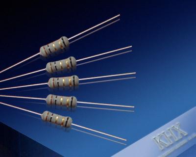
Resistors and types of resistors


types-of-resistors
Whats is a resistance?
The property of a substance, which oppses the flow of an electric current through it is called a resistance. Its is measured in ohms and is represented by letter ‘R’.

Each resistor has two main characteristics.

1) Its resistance value in ohms and 2) its power dissipating capacity in watts
Resistors are employed for many purposes such as electric heaters,telephone equipments, electric and electronic circuit elements and in current limiting devices. As resistors are used in wide applications there values like power rating,R value, tolerance etc vary. Resistors of resistance value ranging from .1ohms to many mega ohms are manufatured. Acceptable tolerance levels range from +/- 20% to as low as +/-.001%. The power rating may be as low as 1/10 watts and can be in several hundred watts. These all vary in range and type of application a particular resistor is used.
Classification of Resistors:
From operating conditions point of view, resistors can be classified into two.
1) Fixed resistors
fixed-resistors
2) Adjustable/ variable resistors

1) Fixed resistors are further classified into:
a) Carbon composition type resistors b) Metalized type resistors c) Wire wound type resistors
a) Carbon composition type resistors:
This is the most common type of low wattage resistor. The resistive material is of carbon-clay composition and the leads are made of tinned copper. These resistors are cheap and reliable and stability is high.
b)Wire wound resistors:
These resistors are a length of wire wound an insulating cylindrical core. Usually wires of material such as constantan (60% copper and 40% nickel) and manganin which have high resistivities and low temperature coefficients are employed. The completed wire wound resistor is coated with an insulating material such as baked enamel.
c) Metalized resistors
It is constructed using film deposition techniques of depositing a thick film of resistive material onto an insulating substrate.Only approximate values of resistance can be had by this method.
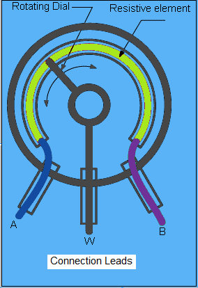
2) Variable resistors
For circuits requiring a resistance that can be adjusted while it remains connected in the circuit(for eg: volume control on radio), variable resistors are required. They usually have 3 lead two fixed and one movable.


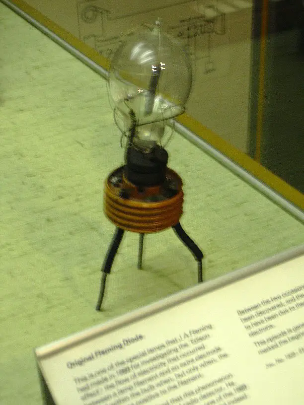
Vacuum tube diodes


fleming-vacuum-diode

Vacuum Diodes-Applications and Construction

The simplest form of the electron tube for the production and control of free electrons is a Vacuum diode. Two electrodes are there for a vacuum diode known as anode and cathode. Cathode serves as an emitter of electrons where as anode serves as a collector of electrons. Cathode may be a simple filament of tungsten or thoriated tungsten. It can also be a nickel tube coated with barium oxide or strontium oxide. Oxide coated cathode shows greater emission efficiency.
Anode is usually a hollow metallic cylinder,it can be of nickel or iron but in case of high power tantalum, molybdenum or graphite may be used. This is because at high power nickel or iron may deteriorate. The anode is made larger to dissipate heat without excessive rise in temperature.Usually cooling fins are fitted with an anode for removal of the heat produced at the anode. Anode surface may be blackened and roughened for the same purpose of easy heat removal.
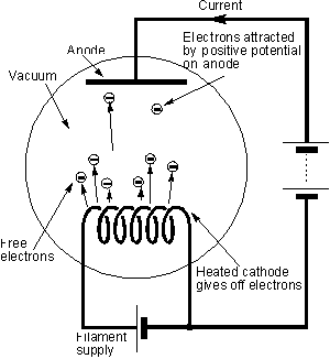
vacuum-diode

Operation of a Vacuum diode:

Basic law of electricity is the basic operating principle of a vacuum diode, which is nothing but “like poles repel and opposite poles attract”. Electrons emitted from cathode are negetive charges, you know that. These negetive charges are either attracted/repelled at the anode,depending on whether the anode is positively/negetively charged.
When a metallic cathode is heated sufficiently an invisible cloud of electrons is set free in the space to form a space charge. The space charge exerts a repelling force on the electrons emitted from cathode. If the anode is made positive w.r.t cathode then an electric field will be created from anode to cathode, and the electrons in the space charge are attracted by the anode and consequently current flows through the tube.
Operation of a Vacuum diode can be simplified as follows:
1) The diode conducts only when the anode or plate is made positive w.r.t  cathode. It will not conduct in opposite direction.
2) Electron flow within diode takes place only from cathode to anode and never from anode to cathode. This unidirectional conduction enables the diode to act like a switch/valve automatically starting or stopping conduction depending upon whether the plate is positive  or negetive respect to cathode. This property permits the diode to act as a rectifier


Tunnel diode


What is a tunnel diode?

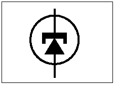
tunnel-diode-symbol
Dr.Leo Esaki invented a tunnel diode, which is also known as “Esaki diode” on behalf of its inventor. Its a high conductivity two terminal P-N junction diode doped heavily about 1000 times greater than a conventional junction diode. Because of heavy doping depletion layer width is reduced to an extremely small value of 1/10000 m. Reverse breakdown voltage is also reduced to very small value~0 resulting in appearance of the diode to be broken for any reverse voltage and a negetive resistance section is produced in the volt-ampere characteristics of the diode.
What is tunneling in a tunnel diode?
Through the reduced depletion layer,it can result in careers “punching through” the junction with velocity of light,even when they have no energy to cross potential barrier. As a result a large forward current is produced at relatively low forward voltage(<100mv). Such a mechanism of conduction in which charge carriers punch through the junction is “tunneling”. Because of heavy doping a tunnel diode cam conduct in both directions but it is usually used for forward conduction only.
Construction of a tunnel diode:
Tunnel diodes are usually fabricated from germanium,gallium arsenide, or gallium antimonide. Silicon is not used in the construction of tunnel diode becuase Ip/Iv is maximum in case of Gallium arsenide.(Ip=Peak value of forward current and Iv= Valley current). This ratio is very small for silicon and is of the order of 3. Ordinarily they are manufatured by alloying from gallium arsenide. Source materials are highly doped semiconductor crystals with an impurity concentration of the order 10^25 per cubic meter.
Note: Being a low power device a tunnel diode can be damaged easily by heat and static electricity.
Tunnel Diode Characteristics is shown below:
tunnel-diode-characteristics

Semiconductor diodes and diode symbol


What is a diode in general?

A two electrode device is called a ‘diode‘. Its simply a P-N junction with connecting leads or terminal on the two sides of the P-N junction. Such diodes are also called a “crystal diode” because the junction is grown out of a crystal. A diode allows unidirectional flow of current and it restrains the flow in opposite direction.
  • Its main advantages are cheapness,smaller size,robustness and high efficiency
  • Major application is rectification which is conversion of ac to dc
A semiconductor diode can be made of either silicon or Germanium. Both differs in size and properties.

Properties of a Silicon diode:

  • Smaller in size compared to Ge diodes
  • Peak Inverse Voltage (PIV) is of 1000 Volts
  • Silicon diodes can be operated above temperatures 200 degree celsius
  • Forward voltage drop is .7 volt
  • Reverse current of a Silicon diode, for a given voltage practically doubles for every 8 degree celsius rise in temperature.

Properties of Germanium Diode:

  • Larger in size compared to Si diode
  • PIV is of 400 volts
  • Operated at temperatures in range 75 to 80 degree celsius
  • Forward voltage drop is .3 volts
  • Reverse current of a Ge diode doubles for every 10 degree celsius rise
Circuit and Graphical symbol of a diode:
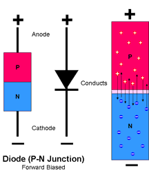
diode-pn junction
diode-pn junction
In the figure given above, first symbol represents the circuit symbol of a semiconductor pn junction diode. The ‘P’ side of diode is always positive terminal and is designated as anode for forward bias. Other side which is negetive is designated as cathode and is the ‘N’ side of diode.
In the figure above, second symbol represents the Graphical symbol of a diode. Direction of the arrow represents the direction of conventional current flow, when the diode is forward biased.

Optoelectronic devices


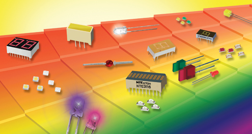
opto_electronic_devices
General Introduction to Opto electronic devices
Optoelectronics is the technology that combines optics and electronics and the devices based on this technology are known as optoelectronic devices. These devices can be catego­rized as light-generating optoelectric devices and light-sensitive devices.. So usually not the kind of thing you can pick up at your local supermarket or o2.co.uk outlet. You might have to try a hardware or electronics store in order to get what you need. Make sure you double check which wattage you require.
The best known types of light-generating optoelectric devices are the ordinary tungsten filament lamp, the light-emitting diode (LED), the multi-segment LED array, and the neon or gas discharge lamp; other types of light-generating devices include the cathode ray tube and the LASER.Light-sensitive devices include photodiodes and phototransistors light sensitive resistors and so-called solar or photovoltaic cells Some specialist de­vices such as optoisolators and optoreflectors combine both light-generating and light-sensi­tive units in a single package. It also include LDR – Light Dependent Resistors , LCD – Liquid Crystal Displays etc.
Applications of Optoelectronic devices
  • They can be employed for generating a wide variety of stationary or moving visual displays.
  • They can be used to provide an automatic switching or alarm action in the presence or absence of a visible or invisible light source
  • They can be employed to provide remote-control action via an infra-red light generator and a remotely placed detector
What is threshold frequency?
Any light source emits energy only over a certain range of frequencies or wavelengths. A graph of energy output plotted against either frequency or wavelength is called the emis­sion spectrum for the light source. A light-sensitive device is sensitive only to a certain range of radiation frequencies. A graph of device current, voltage, or resistance plotted against frequency is known as its spectral response. For a given photosensitive material, there is a minimum radiation frequency (or maximum wavelength) that can produce a photoelectric effect; this frequency is known as the threshold frequency

LDR-Light Dependent Resistors


Electronic optosensors are devices that al­ter their electrical characteristics, in the presence of visible or invisible light. The best known devices of these types are the light dependent resistor (LDR), the photodiode and the phototransistor.
How to make/construction of an LDR
Light dependent resistors (LDRs) are made from cadmium sulphide containing no or very few free electrons when not illuminated. Its resistance is then quite high. When it absorbs light, electrons are liberated and the conductivity of the material increases. Cadmium sulphide (CdS) is, therefore, a photoconductor. The approximate relationship between the resistance and illumination is R = AE~a where E is illumination in lux, R is resist­ance in ohms, A and a are constants. The value of a depends on the cadium sulphide used and on the manufacturing process. Values around 0.7 to 0.9 are quite common.
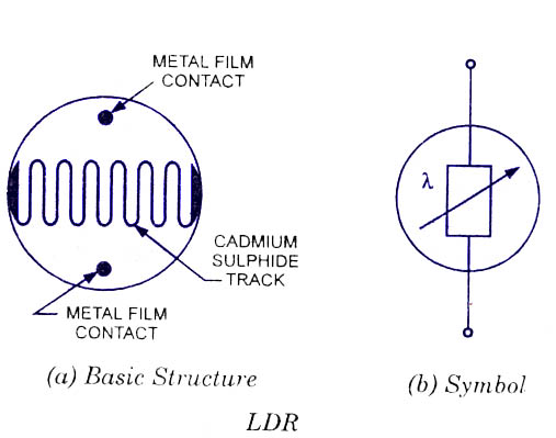
Basic structure of an LDR-Light dependent resistor
ldr-light-dependent-resistor
Device consists of a pair of metal film contacts separated by a snake-like track of cadmium sulphide film, designed to provide the maximum possible contact area with the two metal films. The structure is housed in a clear plastic or resin case, to provide free acess to external light. Practical LDRs are available in a variety of sizes and package styles, the most popular size having a face diameter of roughly 10 mm.
LDRs are sensitive, inexpensive, and readily available devices. They have good power and voltage handling capabilities, similar to those of a conventional resistor. Their only signifi­cant defect is that they are fairly low acting, taking tens or hundreds of milli-seconds to respond to sudden changes in light level. Useful practical applications of LDR include light and dark-activated switches and alarms, light beam alarms and reflective smoke alarms etc

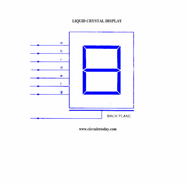
LCD-Liquid Crystal Displays


lcd_liquid-crystal-displays
What is an LCD/Definition of Liquid Crystal Displays
The liquid-crystal display has the distinct advantage of having a low power consumption than the LED. It is typically of the order of microwatts for the display in comparison to the some order of milliwatts for LEDs. Low power consumption requirement has made it compatible with MOS integrated logic circuit. Its other advantages are its low cost, and good contrast. The main drawbacks of LCDs are additional requirement of light source, a limited temperature range of operation (between 0 and 60° C), low reliability, short oper­ating life, poor visibility in low ambient lighting, slow speed and the need for an ac drive.
Basic structure of an LCD
A liquid crystal cell consists of a thin layer (about 10 u m) of a liquid crystal sand­wiched between two glass sheets with transparent elec­trodes deposited on their inside faces. With both glass sheets transparent, the cell is known as transmittive type cell. When one glass is transparent and the other has a reflective coating, the cell is called reflective type. The LCD does not produce any illumination of its own. It, in fact, depends entirely on illumination falling on it from an external source for its visual effect

Types of LCD/Liquid Crystal Displays.

lcd
LCD-Liquid Crystal Displays
Two types of display available are dynamic scatter­ing display and field effect display.
When dynamic scattering display is energized, the molecules of energized area of the display become tur­bulent and scatter light in all directions. Consequently, the activated areas take on a frosted glass appearance resulting in a silver display. Of course, the unenergized areas remain translucent.
Field effect LCD contains front and back polarizers at right angles to each other. Without electrical exci­tation, the light coming through the front polarizer is rotated 90° in the fluid.

Optocoupler devices and application


An optocoupler (or an optoelectronic coupler) is basically an interface between two circuits which operate at (usually) different voltage levels. The key advantage of an optocoupler is the electrical isolation between the input and output circuits. With an optocoupler, the only contact between the input and the output is a beam of light. Because of this it is possible to have an insulation resistance between the two circuits in the thousands of megohms. Isolation like this is useful in high voltage applications where the potentials of two circuits may differ by several thousand volts. 
The most common industrial use of the optocouplers (or optically-coupled isolators) is as a signal converter between high-voltage pitot devices (limit switches etc.) and low voltage solid-state logic circuits. Optical isolators can be employed in any situation where a signal must be passed between two circuits which are isolated from each other. Complete electrical isolation between two circuits (i.e. the two circuits have no conductors in com­mon) is often necessary to prevent noise generated in one circuit from being passed to the other circuit. This is especially necessary for the coupling between high-voltage informa­tion-gathering circuits and low-voltage digital logic circuits. The information circuits are almost badly exposed to noise sources and the logic circuits cannot tolerate noise signals. 
In many applications SCR and triac power circuits are under the control of sensitive electronic systems. For example, it is not unusual to have a microprocessor system pro­grammed to turn motors, lights, and heaters on and off. To reduce the possibility of power-line noise being induced into the control electronics, and to protect it in the event of an SCR or triac failure, it is highly desirable to provide isolation. 
The ideal isolation scheme should only allow signal flow in one direction, should respond to dc levels, and should offer an extremely large resistance between the input and output circuits. These features are available in a class of optoelectronic devices called optocouplers or optoisolators. 
The optical coupling method eliminates the need for a relay-controlled contact or an isolating transformer, which are traditional methods of providing electrical isolation be­tween circuits. The optical coupling method is superior in many applications, because it gets rid of some of the less desirable features of relays and transformers. 
The optocouplers works well on either ac or dc high-voltage signals. For this reason, signal converters employing optical coupling are sometimes referred to the universal signal converters.  
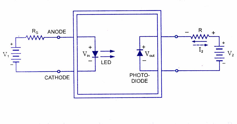
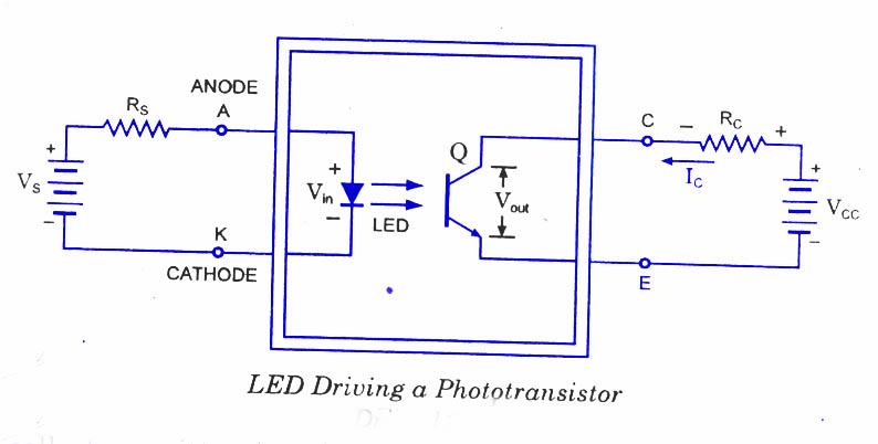
The optocoupler is a device that contains an infra-red LED and a photodetector (such as a photodiode, phototransistor, Darlington pair, SCR or triac) combined in one package. 
optocoupler
optocoupler

An autocoupler combining a LED and a photodiode in a single package is shown in figure. It has a LED on the input side and a photodiode on the output side. The left source voltage and the series resistor set up a current through the LED. Then the. light from the LED impinges on the photo-diode, and this sets up a reverse current in the output circuit. This reverse current develops a voltage across the output resistor R. The output voltage then equals the output supply voltage V2 minus the voltage drop across the load resistor R. When the input voltage is varied, the amount of light fluctuates. 
Types of Optocouplers: 
reflective-slotted-optocoupler

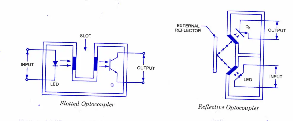
1. Slotted Optocoupler - A slotted optocoupler has a slot moulded into the package between the LED light source and the phototransistor light sensor; the slot houses transparent windows, so that the LED light can normally freely reach the face of transistor , but can be interrupted or blocked via opaque object placed within the slot. The slotted optocoupler can thus be employed in a variety of presence detecting applica­tions, including end-of-tape detection, limit switching, and liquid level detection. 
2. Reflective Optocoupler - Here the LED and phototransistor are optically screened from each other within the package, and both face outwards (in same direction) from the package. The construction is such that an optocoupled link can be set up by a reflective object (such as metallic paint or tape, or even smoke particles) placed a short distance outside the package, in line with both the LED . The reflective coupler can thus be employed in applications such as tape-position detection, en­gine-shaft revolution counting or speed measurement, or smoke or fog detection etc. 
Characteristics of an Optocoupler: 
  
optocoupler-characteristics

  
Current Transfer Ratio (CTR). One of the most important parameters of an optocoupler device is its optocoupling efficiency. This parameter is maximized by closely matching spectrally the LED and the phototransistor (which usually operate in the infra-red range). The optocoupling efficiency of an optocoupler may be conveniently specified by the output-to-input current transfer ratio (CTR) i.e., the ratio of the output current Ic (measured at the collector terminal of the phototransistor), to the input current IF flowing into the LED. 
Input-to-Output Isolation Voltage (Viso). This is the maximum potential difference (dc) that can be allowed to exist between the input and output terminals. Typical values range from 500 V to 4 kV. 
Maximum Collector-Emitter Voltage, VCE (max). This is the maximum allowable dc voltage that can be applied across the output transistor. Typical values may vary from 20 to 80 volts.  
Bandwidth. This is the typical maximum signal frequency (in kHz) that can be use­fully passed through the optocoupler when the device is operated in its normal mode. Typical values vary from 20 to 500 kHz, depending on the type of device construction. 
Response Time. Divided into rise time tr and fall time t*. For a phototransistor output stages, tr and tr are usually around 2 to 5 us. 
A simple isolating optocoupler uses a single phototransistor output stage and is usually housed in a six-pin package, with the base terminal of the phototransistor externally available. In nor­mal use the base is left open circuit, and under such a condition the optocoupler has a minimum CTR value of 20 % and a useful bandwidth of 300 kHz

Photoconductive cells


The photoconductive cell is a two terminal semiconductor device whose terminal resistance will vary (linearly) with the intensity of the inci­dent light. For obvious reasons, it is frequently called a photoresistive device.
The photoconductive materials most frequently used include cadmium sulphide (CdS) and cadmium selenide (CdSe). Both materials respond rather slowly to changes in light intensity. The peak spectral response time of CdS units is about 100 ms and 10 ms for CdSe cells. Another im­portant difference between the two materials is their temperature sensitivity. There is large change in the resistance of a cadmium selenide cell with changes in ambient temperature, but the re­sistance of cadmium sulphide remains relatively stable. The spectral response of a cadmium sulphide cell closely matches thatof the human eye, and the cell is therefore often used in applications where human vision is a factor, such as street light control or automatic iris control for cameras.
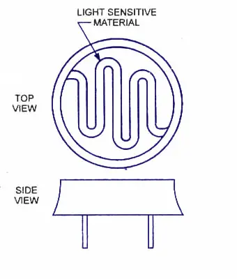
The essential elements of a photoconductive cell are the ceramic substrate, a layer of photo­conductive material, metallic electrodes to connect the device into a circuit and a moisture re­sistant enclosure.
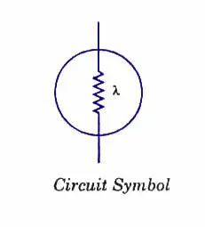
The circuit symbol and construction of a typical photoconductive cell are shown.


photo-conductive-cell-circuit-symbol
photo-conductive-cell-construction

Light sensitive material is arranged in the form of a long strip, zigzagged across a disc shaped base with protective sides. For added protection, a glass or plastic cover may be included. The two ends of the strip are brought out to connecting pins below the base.
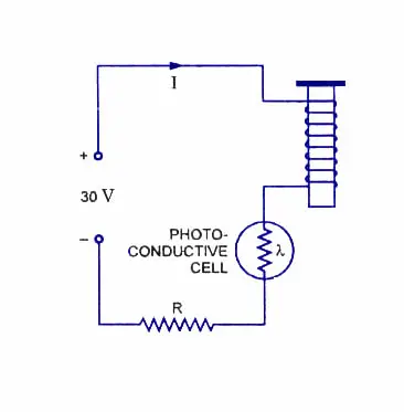
Photoconductive cell circuit:
photo-conductive-cell-circuit
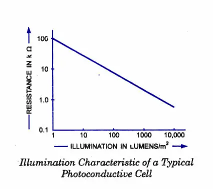
Characteristics of a Photoconductive cell:


photo-conductive-cell-characteristics
The illumination characteristics of a typi­cal photoconductive cell are shown from which it is obvious that when the cell is not illuminated its resistance may be more than 1 00 kilo ohms. This resistance is called the dark resistance. When the cell is illumi­nated, the resistance may fall to a few hun­dred ohms. Note that the scales on the illu­mination characteristic are logarithmic to cover a wide ranges of resistance and illu­mination that are possible. Cell sensitivity may be expressed in terms of the cell cur­rent for a given voltage and given level of illumination.
The major drawback of the photoconduc­tive cells is that temperature variations cause substantial variations in resistance for a substantial variations in resistance for a particular light intensity. Therefore such a cell is unsuitable for analog applications.
The photoconductive cell used for relay control is shown as circuit above When the cell is il­luminated, its resist­ance is low and the relay current is at its maximum. When the cell is dark, its high resistance re­duces the current down to a level too low to energize the relay. Resistance R is included to limit the relay current to the desired level when the resistance of the cell is low. Photoconductive cells are used to switch transistors on and off, as illustrated in figure. When the cell shown in figure is dark, the transistor base is biased above its emitter level, and the device is turned on. When the cell is illuminated, the lower resist­ance of the cell in series with R biases the transistor base voltage below its emitter level. Thus, the device is turned off.

Fabrication techniques of a P-N junction diode


General Introduction to Fabrication techniques of a P-N junction diode:
pn-junction-fabrication
In practice, the P-N junction is formed from a single mono crystalline structure by adding carefully controlled amounts of donor and acceptor impurities. Here discussion is limited only to acquaintation with the basic techniques and terminology (not expertise in fabrication).
The first and foremost requirement is to obtain an extremely pure germanium or silicon. Impurity of less than one part in ten billion (1010) is required for most semiconductor device fabrication to-day. For obtaining pure semiconductor material it is first purified chemically. For reducing the impurities further, and to ensure the formation of a mono crystalline structure, a technique known as flatting zone is quite often employed.The mono crystalline structure is formed through the use of a small seed of semiconductor (e.g., silicon or germanium). The seed itself is a monocrystal that has been very carefully cut along the face of its cubic lattice. Support clamps are employed to hold the low-purity polycrystalline rod.
The rod, seed, and support clamps are placed in a quartz cylinder. The process may be carried out in vacuum or by surrounding the semiconductor with an inert gas. Great care is required to ensure that the semiconductor is not further contaminated during the floating zone process.
Induction coils encompass the quartz container, as shown in figure. The coils are excited by a radio-frequency voltage. Circulating currents are induced in the semiconductor due to the magnetic field set up by RF currents flowing through the induction coils. The heat so produced melts the zone which is exposed to it. As a result, a molten region is formed.
Slow rotation of rod makes the semiconductor atoms to align themselves with the atoms in the monocrystalline seed. Thus as the induction coils are moved downward, the molten region follows, and a monocrystalline structure continues to grow from the seed. Purification of the semiconductor rod occurs simultaneously with the formation of the monocrystal. The impurities in the semiconductor rod tend to become ‘more liquid’ than the semiconductor. Thus as the induction coils are moved downward, the impurities tend to follow the molten region. Once the induction coils have traversed the length of the semiconductor rod, the impurities are collected in its lower end. The lower end of the semiconductor rod may then be cut off, and the process is repeated until the desired impurity level is attained.
Once a pure monocrystalline semiconductor has been produced, carefully controlled I amount of donor and acceptor impurities are added to the semiconductor without disturbing the orderly monocrystalline structure. Thus a P-N junction is formed.
Semiconductor diodes are normally one of the following types:
1. Grown junction diode
2. Alloy type or fused junction diode
3. Diffused junction diode
4. Epitaxial grown or planar diffused diode
5. Point contact diode

Semiconductor diode fabrication types


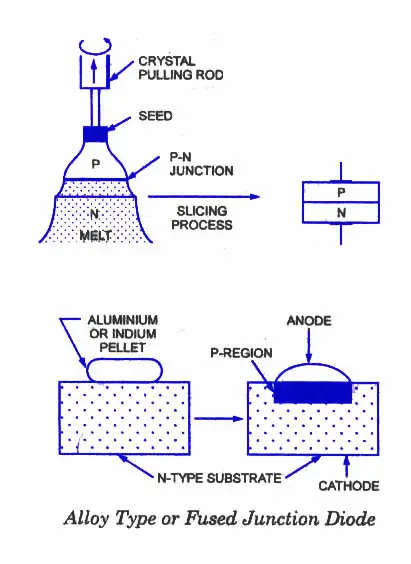
1. Grown Junction Diode: Diodes of this type are formed during the crystal pulling process. P and N-type impurities can be alternately added to the molten semiconductor material in the crucible, which results in a P-N junction, as shown when crystal is pulled. After slicing, the larger area device can then be cut into a large number (say in thousands) of smaller-area semiconductor diodes. Though such diodes, because of larger area, are capable of handling large currents but larger area also introduces more capacitive effects, which are undesirable. Such diodes are used for low frequencies.
2. Alloy Type or Fused Junction Diode: Such a diode is formed by first placing a P- type impurity (a tiny pellet of aluminium or some other P- type impurity) into the surface of an N-type crystal and heating the two until liquefaction occurs where the two materials meet. An alloy will result that on cooling will give a P-N junction at the boundary of the alloy substrate. Similarly, an N-type impurity may be placed into the surface of a P- type crystal and the two are heated until liquefaction occurs. Alloy type diodes have a high cur­rent rating and large PIV (peak inverse voltage) rating. The junction capacitance is also large, due to the large junction area.
alloy-type or fused junction diode
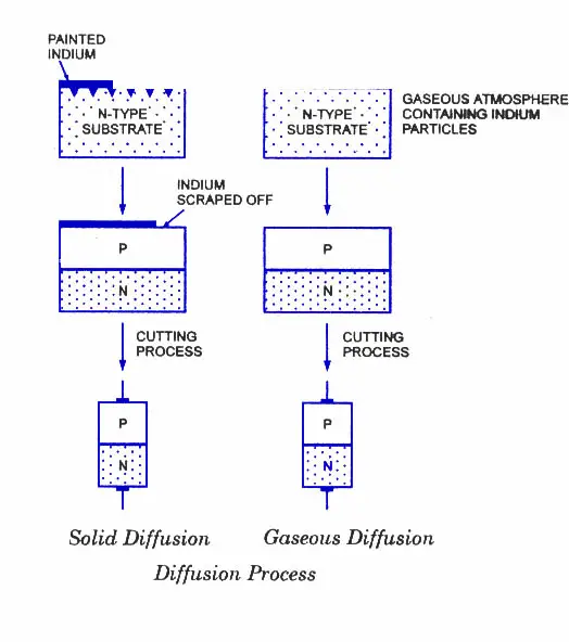
3. Diffused Junction Diode: Diffu­sion is a process by which a heavy con­centration of particles diffuse into a sur­rounding region of lower concentration. The main difference between the diffu­sion and alloy process is the fact that liquefaction is not reached in the diffu­sion process. In the diffusion process heat is applied only to increase the activity of elements involved. For formation of such diodes, either solid or gaseous diffusion process can be employed. The process of solid diffusion starts with formation of layer of an acceptor impurity on an N- type substrate and heating the two until the impurity diffuses into the substrate to form the P-type layer, as illustrated in figure. A large P-N junction is divided into parts by cutting process. Metallic contacts are made for connecting anode and cathode leads.
In the process of gaseous diffusion instead of layer formation of an acceptor impurity, an N- type substrate is placed in a gaseous atmosphere of acceptor impurities and then heated. The impurity diffuses into the substrate to form P- type layer on the N- type substrate. Though, the diffusion process requires more time than the alloy process but it is relatively inexpensive, and can be very accurately controlled. The diffusion technique leads itself to the simultaneous fabrication of many hundreds of diodes on one small disc of semiconductor material and is most commonly used in the manufacture of semiconductor diodes. This technique is also used in the production of transistors and ICs (integrated circuits).
diffused-junction-diode
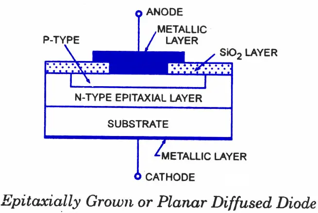
4. Epitaxial Growth or Planar Diffused Diode. The term “epitaxial” is derived from the Latin terms epi meaning ‘upon’ and taxis meaning “arrangement”.To construct an epitaxially grown diode, a very thin (single crystal) high impurity layer of semiconductor material (silicon or germanium) is grown on a heavily doped substrate (base) of the same material. This complete structure then forms the N- region on which P- region is diffused. Si02 layer is thermally grown on the top surface, photo-etched and then aluminium contact is made to the P- region. A metallic layer at the bottom of the substrate forms the cathode to which lead is attached.This process is usually employed in the fabrication of IC chips.
epitaxially-grown-diode
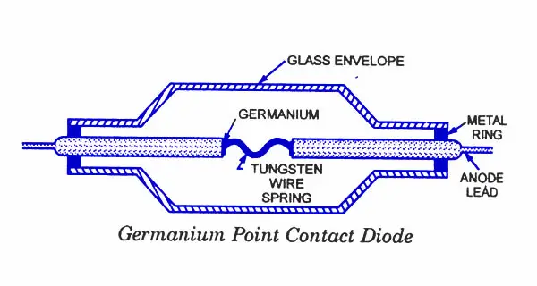
5. Point Contact Diode. It consists of an N-type germanium or silicon wafer about 12.5 mm square by 0.5 mm thick, one face of which is soldered to a metal base by radio-frequency heating and the other face has a phosphor bronze or tung­sten spring pressed against it. A barrier layer is formed round the point contact by a pulsating current forming process. This causes a P-region to be formed round the wire and since pure germanium is N-type, a very small P-N junction in the shape of a hemisphere is formed round the point contact. The forming process cannot be controlled with precision. Because of small area of the junction, point contact diode can be used to rectify only very small currents (of the order of m A). On the other hand, the shunting capacitance of point contact diodes are very valuable in equipment operating at super high frequencies (as high as 25,000 MHz).
point-contact-diode
point-contact-diode

Page Rank

google pagerank

Write For Us

Submit a Guest Post

Find us on Facebook

Categories

555 Timer IC 7 segment Display 8051 Project AC Circuits Adafruit Alarms Amplifier Circuits Analog Circuits android Arduino arm processor Assembly Languange Atmel Atom Size Audio Circuits augmented reality Automotive Circuits avr Battery Circuits Bicycle Gurad bluetooth Cable TV Circuits Cambridge University Camera Technology Circuit Boards Clipping And Clamping Circuits Clocking And Timer Circuits Computing contact lens Contact Us Form Contests Controller Circuit Conversion Circuits Counter Circuits Digital Electronics diy circuits Downloads EFY EFYTimes Electronic Books Electronic Components Electronic Locks And Keys Engineering Fan Circuits Filter Circuits Fire Alarm free Frequency Fun And Game Circuits future Google Hack n Mod Ham Radio Circuits heart rate monitoring High Voltage Circuits Home Circuits IC Guide ieee Industrial Circuits Infrared Instructables Inventions ipad lcd Led Circuits Light Related Lighting Circuits Medical Circuits Meter Clocks Microcontrollers Microprocessors Mini Projects modules Movie maker NatGeo Navigation Notice Optical Fiber PC Circuits PCB Boards Physics pnp transistor Power Supplies Printing Projects Programmer Project Ideas Projectors Protection circuits Proximity Detectors Radar Radio Circuits Radio Transmitters Raspberry Raspberry Pie Remote Circuits Retis Lab RFID Robot Cars Robotics Science Science Alert Security And Safety Sensor Circuits Servo Motors Smallest Smartwatches sms Software solar cell sound application Spectram Switch Technology News Telephone Related Television Related Test And Measurement Circuits Thermal Projects Tone generator circuits Touch Screen Tutorials Wearables Wi-Fi Wireless
Like us on Facebook
Follow us on Twitter
Recommend us on Google Plus
Subscribe me on RSS