Search This Blog

Powered by Blogger.

Translate

[TC] Bicycle Theft Guard

This antitheft device for bicycles is inexpensive and can be constructed easily using a few components.

At the heart of the circuit is a wheel rotation detector, realised using a DC micro motor. For the purpose, you can use the micromotor (spindle motor) of a discarded local CD deck mechanism. With a little skill and patience, you can easily attach a small metallic pulley covered with a rubber washer to the motor spindle. Thereafter, fix the unit in the back wheel of the cycle, like the existing dynamo assembly.


Power supply switch S1 should be kept ‘on’ when you are using this bicycle guard. When it is flipped towards ‘on’ position, the circuit gets power from the miniature 12V battery. Now LED1 lights up and resistor R4 limits the LED current. Next, the monostable built around IC1, which is CMOS version of timer LM555, is powered through a low-current, fixed-voltage regulator IC2 (78L05).

Initially, when the bicycle is standing still, the monostable output at pin 3 of IC1 is low and the circuit is in idle state. In the event of a theft attempt, forward or reverse rotation of the DC motor induces a small voltage at its DC input terminals and the internal LED of 4-pin DIP AC input isolator optocoupler IC3 (PS2505-1 or PC814) glows. As a result, the internal transistor of IC3 conducts and pin 2 of IC1 is pulled low by the optocoupler and the monostable built around IC1 is triggered.

The output at pin 3 of IC1 now drives piezobuzzer-driver transistor T1 via resistor R3 and the buzzer starts sounding to alert you. In this circuit, the buzzer remains ‘on’ for around two minutes. You can change this time by changing the values of resistor R2 and capacitor C1.

Zener diodes ZD1 and ZD2 (each 5.1V) act as a protector for optocoupler IC3. The costly GP12V/27A battery is used here due to its compact size and reliability. 12V active buzzers with high-pitched tone output may be used with this circuit. These are readily available in the market.

Note. The specific optocoupler is used here deliberately, instead of a bridge rectifier, to increase the circuit’s detection sensitivity. Never replace the same with a DC optocoupler


Source : http://electronicsforu.com/

Tutorial: Making Solar Cell Using 2N3055 Transistor


This video unveils the fact that a silicon diode is quite similar to a solar cell. To prove this, it takes apart a 2N3055 power transistor to produce 1.6 milliwatts. Watch the video for a great tutorial on creating a transistor solar cell.

It's easy to cut open a power transistor like the 2N3055 to expose the NPN silicon material inside to make a solar cell. When exposed to sunlight, or household lights, it conducts electricity. The N-type and P-type materials work like a solar cell. The best way is from the Base to the Collector though from both the Base and Emitter combined and then to the Collector also works well. The voltage and current aren't much but with just a few of them in series you can power a small 1.5 volt calculator.


Source: http://electronicsforu.com/newelectronics/video/detailvideo.asp?id=2077

[TC] Multifunction Power Supply

Many embedded systems these days need +5V power supply with some special functions such as power-fail detection, zero-crossing signals for mains power supply and possibility to maintain the charging of built-in batteries. 

Presented here is the circuit of such a power supply for embedded systems. It provides +5V, battery charger, zero-crossing signals and power-fail signal. The circuit is based on popular low-cost components. It needs simple adjustment with potmeter POT1 to immediately get you started.

Circuit and working
The circuit shown in Fig. 1 is built around a step-down transformer (X1), two bridge rectifiers(BR1 and BR2), adjustable voltage regulator LM317 (IC1), 5V voltage regulator 7805 (IC2), hex inverter Schmitt trigger 74HC14 (IC3) and a few discrete components. 


Fig. 1: Circuit of multifunction power supply 
The mains power supply 230V AC, 50Hz is applied to connector CON1. Fuse F1 protects the input from overloads. Resistor R1 and capacitor C1 filter some of the noise coming from the mains power supply. The secondary of power transformer X1 is 12V, 2.5A.

CON3 provides +5V, 1A power supply using standard 5V regulator IC2. Rectifying bridge BR1 is of 2.5A. The value of the main filtering capacitor (C4) should be at least 4700 µF. IC2 provides regulated +5V with output current up to 1A. If a higher current is needed, regulators like 78T05 (3A, 5V) or 78S05 (2A, 5V) can be used. In practice, it is better to limit the load for 78XX up to around 0.7-0.8A. The unregulated output at CON4 provides voltage of 10V to 18V depending on the transformer used and the current consumption from the power supply. This unregulated voltage can be used for peripheral functions. Fuse F2 is used to protect the output.

The power supply incorporates battery charger with adjustable regulator IC1. A 6V rechargeable battery is used to provide power supply to some parts of the system when the mains power supply does not function properly. The maximum voltage level across the rechargeable battery is adjusted using potmeter POT1. The maximum charging current is limited by resistor R7. Regulator IC1 can provide output voltage of +1.25V to +8.2V,  adjustable with potmeter POT1.

Diodes D1, D2 and D3 protect regulators IC1 and IC2. Bridge rectifier BR2 is used only to provide signals around the zero crossings. Capacitor C2 should have a small value. It is intended to cut only the very high frequency, not to filterthe mains power supply. The values of R2 and R3 can be changed depending on IC3 and parameters of the produced pulses.

CON5 provides power-fail signal when the voltage at test point TP2 falls below approximately 8V. Transistor T1 stops conducting and the control unit is intimated the same by a high signal at pin 3 of CON5.

The threshold voltage of the power-fail signal is regulated with zener diode ZD2 (7.5V) and resistors R4 and R5. Transistor T1 should preferably be switching type, but most of the npn silicon transistors with a high gain will also work well.

The outputs from pins 2, 3 and 4 of connector CON6 provide different signals with a frequency that is double the frequency of the mains power supply (100 Hz). These signals are active near zero crossings of the mains power supply and can be used for several purposes, such as: 

1. The control unit can use them to measure the frequency of the mains power supply.
2. These can be used to synchronise the operation of the control unit with zero crossings of the mains power supply.
3. Тhe amplitude of signal TP4 is proportional to the secondary voltage of the transformer. The control unit can measure it and determine the secondary voltage of X1. 
4. Outputs TP5 and TP3 are TTL- or CMOS-compatible depending on IC3. IC3 can be CMOS or TTL; e.g., 74HC14, 74HCT14, 74LS14, etc. It should have built-in Schmitt trigger. 

Construction and testing
Use individual heat-sinks for IC1 and IC2. The size of the heat-sink should be calculated according to the dissipated heat for each particular case; e.g., the thermal resistance should be below 5°C/W for each heat-sink. The metallic part of 7805 is connected to the ground pin, while the metallic part of LM317 is connected to the output pin. 


Fig. 2: An actual-size, single-side PCB for the multifunction power supply


Fig. 3: Component layout for the PCB 
Download: http://www.electronicsforu.com/


An actual-size, single-side PCB for the multifunction power supply is shown in Fig. 2 and its component layout in Fig. 3. After assembling the circuit on a PCB, enclose it in a suitable case. Fix all the connectors at the rear side of the cabinet for connecting the mains and taking the outputs. 

To test the circuit, switch on switch S1 and check various voltages as indicated in the test-points table. LED1 indicates the availability of 5V.

Source: http://electronicsforu.com

[TC] Multifunction Power Supply

Many embedded systems these days need +5V power supply with some special functions such as power-fail detection, zero-crossing signals for mains power supply and possibility to maintain the charging of built-in batteries. 
Presented here is the circuit of such a power supply for embedded systems. It provides +5V, battery charger, zero-crossing signals and power-fail signal. The circuit is based on popular low-cost components. It needs simple adjustment with potmeter POT1 to immediately get you started.

Circuit and working
The circuit shown in Fig. 1 is built around a step-down transformer (X1), two bridge rectifiers(BR1 and BR2), adjustable voltage regulator LM317 (IC1), 5V voltage regulator 7805 (IC2), hex inverter Schmitt trigger 74HC14 (IC3) and a few discrete components. 


Fig. 1: Circuit of multifunction power supply 
The mains power supply 230V AC, 50Hz is applied to connector CON1. Fuse F1 protects the input from overloads. Resistor R1 and capacitor C1 filter some of the noise coming from the mains power supply. The secondary of power transformer X1 is 12V, 2.5A.

CON3 provides +5V, 1A power supply using standard 5V regulator IC2. Rectifying bridge BR1 is of 2.5A. The value of the main filtering capacitor (C4) should be at least 4700 µF. IC2 provides regulated +5V with output current up to 1A. If a higher current is needed, regulators like 78T05 (3A, 5V) or 78S05 (2A, 5V) can be used. In practice, it is better to limit the load for 78XX up to around 0.7-0.8A. The unregulated output at CON4 provides voltage of 10V to 18V depending on the transformer used and the current consumption from the power supply. This unregulated voltage can be used for peripheral functions. Fuse F2 is used to protect the output.

The power supply incorporates battery charger with adjustable regulator IC1. A 6V rechargeable battery is used to provide power supply to some parts of the system when the mains power supply does not function properly. The maximum voltage level across the rechargeable battery is adjusted using potmeter POT1. The maximum charging current is limited by resistor R7. Regulator IC1 can provide output voltage of +1.25V to +8.2V,  adjustable with potmeter POT1.

Diodes D1, D2 and D3 protect regulators IC1 and IC2. Bridge rectifier BR2 is used only to provide signals around the zero crossings. Capacitor C2 should have a small value. It is intended to cut only the very high frequency, not to filterthe mains power supply. The values of R2 and R3 can be changed depending on IC3 and parameters of the produced pulses.

CON5 provides power-fail signal when the voltage at test point TP2 falls below approximately 8V. Transistor T1 stops conducting and the control unit is intimated the same by a high signal at pin 3 of CON5.

The threshold voltage of the power-fail signal is regulated with zener diode ZD2 (7.5V) and resistors R4 and R5. Transistor T1 should preferably be switching type, but most of the npn silicon transistors with a high gain will also work well.

The outputs from pins 2, 3 and 4 of connector CON6 provide different signals with a frequency that is double the frequency of the mains power supply (100 Hz). These signals are active near zero crossings of the mains power supply and can be used for several purposes, such as: 

1. The control unit can use them to measure the frequency of the mains power supply.
2. These can be used to synchronise the operation of the control unit with zero crossings of the mains power supply.
3. Тhe amplitude of signal TP4 is proportional to the secondary voltage of the transformer. The control unit can measure it and determine the secondary voltage of X1. 
4. Outputs TP5 and TP3 are TTL- or CMOS-compatible depending on IC3. IC3 can be CMOS or TTL; e.g., 74HC14, 74HCT14, 74LS14, etc. It should have built-in Schmitt trigger. 

Construction and testing
Use individual heat-sinks for IC1 and IC2. The size of the heat-sink should be calculated according to the dissipated heat for each particular case; e.g., the thermal resistance should be below 5°C/W for each heat-sink. The metallic part of 7805 is connected to the ground pin, while the metallic part of LM317 is connected to the output pin. 


Fig. 2: An actual-size, single-side PCB for the multifunction power supply


Fig. 3: Component layout for the PCB 
Download: Click Here
An actual-size, single-side PCB for the multifunction power supply is shown in Fig. 2 and its component layout in Fig. 3. After assembling the circuit on a PCB, enclose it in a suitable case. Fix all the connectors at the rear side of the cabinet for connecting the mains and taking the outputs. 

To test the circuit, switch on switch S1 and check various voltages as indicated in the test-points table. LED1 indicates the availability of 5V.


Source : http://electronicsforu.com/

Mini UPS


Here the simple Mini UPS circuit diagram. This circuit can provide an uninterrupted power supply (UPS) to operate 12V, 9V and 5V DC-powered instruments at up to 1A current. The backup battery will take up the load with no spikes or delay when the mains electrical power gets interrupted. It could possibly also be utilized as a workbench power supply that delivers 12V, 9V and 5V operating voltages. The circuit instantly disconnects the load when the battery voltage decreases to 10.5V to avoid deep discharge of your battery. LED1 indication is presented to indicate the complete charge voltage level of the battery. Miniature white LEDs (LED2 and LED3) are utilized as emergency lamps especially during electrical power failure at night time.
A common step-down transformer delivers 12V of AC, that is rectified by diodes D1 and D2. Capacitor C1 features ripple-free DC to charge the battery and to the remaining circuit. When the mains electrical power is on, diode D3 gets forward biased to charge the battery. Resistor R1 limits the charging current. Potentiometer VR1 (10k) with transistor T1 acts as being the voltage comparator to indicate the voltage level. VR1 is so adjusted that LED1 is in the ‘off’ mode. when the battery is completely charged, LED1 glows indicating a maximum voltage level of 12V.
Download the circuit diagram of Mini UPS and full explanation about how it’s work, download this PDF file:
» Download Link

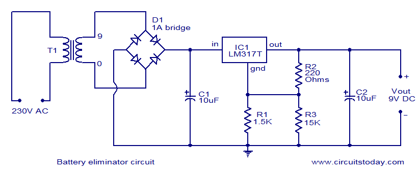
Battery eliminator circuit


Description.
Here is the circuit diagram of a battery eliminator circuit that can be used as a replacement for 9V PP3 batteries. The circuit given here can be used to power any device that operates from a 9V battery. The transformer T1 steps down the mains voltage and bridge D1 performs the job of rectification. Capacitor C1 is a filter. IC LM317T is the regulator here. The value of R1, R2 and R3 are so selected that the output voltage of IC1 will be steady 9 volts.
Circuit diagram.
battery eliminator circuit
Notes.
  • Assemble the circuit on a good quality PCB.
  • Transformer T1 can be a 230V primary, 9V secondary, 1.5A step down transformer.
  • If 1A Bridge is not available, then make one using four 1N 4007 diodes.
  • Do not connect loads that consume more than 1.5A to this circuit.
  • A heat sink is recommended for IC1

Page Rank

google pagerank

Write For Us

Submit a Guest Post

Find us on Facebook

Categories

555 Timer IC 7 segment Display 8051 Project AC Circuits Adafruit Alarms Amplifier Circuits Analog Circuits android Arduino arm processor Assembly Languange Atmel Atom Size Audio Circuits augmented reality Automotive Circuits avr Battery Circuits Bicycle Gurad bluetooth Cable TV Circuits Cambridge University Camera Technology Circuit Boards Clipping And Clamping Circuits Clocking And Timer Circuits Computing contact lens Contact Us Form Contests Controller Circuit Conversion Circuits Counter Circuits Digital Electronics diy circuits Downloads EFY EFYTimes Electronic Books Electronic Components Electronic Locks And Keys Engineering Fan Circuits Filter Circuits Fire Alarm free Frequency Fun And Game Circuits future Google Hack n Mod Ham Radio Circuits heart rate monitoring High Voltage Circuits Home Circuits IC Guide ieee Industrial Circuits Infrared Instructables Inventions ipad lcd Led Circuits Light Related Lighting Circuits Medical Circuits Meter Clocks Microcontrollers Microprocessors Mini Projects modules Movie maker NatGeo Navigation Notice Optical Fiber PC Circuits PCB Boards Physics pnp transistor Power Supplies Printing Projects Programmer Project Ideas Projectors Protection circuits Proximity Detectors Radar Radio Circuits Radio Transmitters Raspberry Raspberry Pie Remote Circuits Retis Lab RFID Robot Cars Robotics Science Science Alert Security And Safety Sensor Circuits Servo Motors Smallest Smartwatches sms Software solar cell sound application Spectram Switch Technology News Telephone Related Television Related Test And Measurement Circuits Thermal Projects Tone generator circuits Touch Screen Tutorials Wearables Wi-Fi Wireless
Like us on Facebook
Follow us on Twitter
Recommend us on Google Plus
Subscribe me on RSS