Search This Blog

Powered by Blogger.

Translate

[TC News] New laser promises to make internet faster

Scientists have developed a new laser
that holds the potential to increase by
orders of magnitude the rate of
data transmission on the internet.

WASHINGTON: Scientists have developed a new laser that holds the potential to increase by orders of magnitude the rate of data transmission in the optical-fibre network - the backbone of the internet. 

The laser is the result of a five-year effort by researchers at the California Institute of Technology (Caltech). 

Light is capable of carrying vast amounts of information - approximately 10,000 times more bandwidth than microwaves, the earlier carrier of long-distance communications. 

To utilize this potential, the laser light needs to be as spectrally pure - as close to a single frequency - as possible. The purer the tone, the more information it can carry, and researchers have been trying to develop a laser that comes as close as possible to emitting just one frequency. 

Today's worldwide optical-fibre network is still powered by a laser known as the distributed-feedback semiconductor (S-DFB) laser, developed in mid-1970s, researchers said. 


The S-DFB laser's unusual longevity in optical communications stemmed from its, at the time, unparallelled spectral purity - the degree to which the light emitted matched a single frequency. 

The S-DFB laser managed to attain such purity by using a nanoscale corrugation within the laser's structure that acts like a filter. 

Although the old S-DFB laser had a successful 40-year run in optical communications, the spectral purity, or coherence, of the laser no longer satisfies the ever-increasing demand for bandwidth, researchers said. 

The old S-DFB laser consists of continuous crystalline layers of materials called III-V semiconductors - typically gallium arsenide and indium phosphide - that convert into light the applied electrical current flowing through the structure. 

Since III-V semiconductors are also strong light absorbers - and this absorption leads to a degradation of spectral purity - the researchers sought a different solution for the new laser. 

The high-coherence new laser still converts current to light using the III-V material, but in a fundamental departure from the S-DFB laser, it stores the light in a layer of silicon, which does not absorb light. 

Spatial patterning of this silicon layer - a variant of the corrugated surface of the S-DFB laser - causes the silicon to act as a light concentrator, pulling the newly generated light away from the light-absorbing III-V material and into the near absorption-free silicon. 

This newly achieved high spectral purity - a 20 times narrower range of frequencies than possible with the S-DFB laser - could be especially important for the future of fibre-optic communications, researchers said. 

The study was published in the Proceedings of the National Academy of Sciences.


Source: http://timesofindia.indiatimes.com

[TC] Home Made Movie Maker

Like real movies, this circuit makes use of a characteristic of the human eye and brain known as the persistence of vision. A sequence of still pictures is projected onto a screen in rapid succession. The pictures differ slightly from one another and the brain interprets the succession of still pictures as continuous motion.
Here the pictures are shadows cast by low-voltage lamps. There are four Lamps in all, which glow in sequence cyclically. This gives the illusion of a simple but realistic movie.

Fig. 1 shows the circuit for the movie maker. It is driven by clock pulses provided by NAND gates N1 and N2. The flickering frequency is adjustable through preset VR1. A suitable rate for perceiving continuous motion is 16 Hz. The clock pulses are fed to counter IC CD4022 (IC2). IC2 has eight outputs, but only the first four (0-3) are used in this circuit. The outputs go high one at a time, in sequence. The fifth output (output 4) is connected to the reset input so that the counter is immediately reset at the fifth count and the first output (output 0) goes high.

The counter outputs are fed to CD4049 hex buffer (IC3). The buffer outputs drive transistors T1 through T4 in a sequence. As each transistor conducts, the lamp connected to it glows. The lamps are rated at 0.3A so these provide enough light to operate the movie show in a dimly-lit room.

Fig. 1: Circuit for movie maker

Assemble the circuit on a general-purpose PCB. Power-on the circuitusing switch S1 and make sure that the outputs of IC2 (0 through 3) are normally low but briefly go high three-four times within a second. Also ensure that the lamps flash one at a time in a repeating sequence. If the sequence appears to be wrong or any of the lamps fails to glow, check the wiring. The light shield and film holder can be made of a thin card, sheet metal or plywood. Strictly adhere to the various dimensions as shown in Fig. 2. Otherwise, the shadow images may fail to register properly when projected.

Use a plastic cabinet as shown in Fig. 3 to hold the circuit board and battery. Owing to the power requirements of the lamps, it is more economical to use four 1.5V cells in a battery box. Else, you can use a 6V power adaptor. 


Fig. 2: Assembly arrangement

There are two ways of mounting the lamps. The more satisfactory but more expensive method is to bolt the four lamps. Alternatively, drill four 1cm dia. holes on the front of the cabinet, wedge the base of the lamps in these holes and solder wire to the bases.


Fig. 3: Plastic case with assembled circuit 

The easiest way to prepare the film frames is to photocopy the desired drawings onto transparent films. Alternatively, trace them on a transparent acetate film or draughtsman's film, using a fine marker pen. Align all the drawings on the frames and project onto the screen. 

  
Fig. 3: Flim making

Working of the circuit is simple. First of all, fix the clock frequency at about 16 Hz. Place the film on the holder. Ensure a distance of 12 cm between the screen and the assembled unit and power-on the circuit using switch S1. Now you can see your drawings as a short movie clip on the screen.

EFY note. We have tested this circuit without the mechanical arrangement.


Source: 
  http://electronicsforu.com/

[TC] Bicycle Theft Guard

This antitheft device for bicycles is inexpensive and can be constructed easily using a few components.

At the heart of the circuit is a wheel rotation detector, realised using a DC micro motor. For the purpose, you can use the micromotor (spindle motor) of a discarded local CD deck mechanism. With a little skill and patience, you can easily attach a small metallic pulley covered with a rubber washer to the motor spindle. Thereafter, fix the unit in the back wheel of the cycle, like the existing dynamo assembly.


Power supply switch S1 should be kept ‘on’ when you are using this bicycle guard. When it is flipped towards ‘on’ position, the circuit gets power from the miniature 12V battery. Now LED1 lights up and resistor R4 limits the LED current. Next, the monostable built around IC1, which is CMOS version of timer LM555, is powered through a low-current, fixed-voltage regulator IC2 (78L05).

Initially, when the bicycle is standing still, the monostable output at pin 3 of IC1 is low and the circuit is in idle state. In the event of a theft attempt, forward or reverse rotation of the DC motor induces a small voltage at its DC input terminals and the internal LED of 4-pin DIP AC input isolator optocoupler IC3 (PS2505-1 or PC814) glows. As a result, the internal transistor of IC3 conducts and pin 2 of IC1 is pulled low by the optocoupler and the monostable built around IC1 is triggered.

The output at pin 3 of IC1 now drives piezobuzzer-driver transistor T1 via resistor R3 and the buzzer starts sounding to alert you. In this circuit, the buzzer remains ‘on’ for around two minutes. You can change this time by changing the values of resistor R2 and capacitor C1.

Zener diodes ZD1 and ZD2 (each 5.1V) act as a protector for optocoupler IC3. The costly GP12V/27A battery is used here due to its compact size and reliability. 12V active buzzers with high-pitched tone output may be used with this circuit. These are readily available in the market.

Note. The specific optocoupler is used here deliberately, instead of a bridge rectifier, to increase the circuit’s detection sensitivity. Never replace the same with a DC optocoupler


Source : http://electronicsforu.com/

[TC] Automatic Street Light

Introduction:
Needs no manual operation for switching ON and OFF. When there is need of light it automatically switches ON. When darkness rises to a certain value then sensor circuit gets activated and switches ON and when there is other source of light i.e. day time, the street light gets OFF. The sensitiveness of the street light can also be adjusted. In our project we have used four L.E.D for indication of bulb but for high power switching one can connect Relay (electromagnetic switch) at the output of pin 3 of I.C 555. Then it will be possible to turn ON/OFF any electrical appliances connected all the way through relay.

                        Automatic Street Light
Principle :
This circuit uses a popular timer I.C 555. I.C 555 is connected as comparator with pin-6 connected with positive rail, the output goes high(1) when the trigger pin 2 is at lower then 1/3rd level of the supply voltage. Conversely the output goes low (0) when it is above 1/3rd level. So small change in the voltage of pin-2 is enough to change the level of output (pin-3) from 1 to 0 and 0 to 1. The output has only two states high and low and can not remain in any intermediate stage. It is powered by a 6V battery for portable use. The circuit is economic in power consumption. Pin 4, 6 and 8 is connected to the positive supply and pin 1 is grounded. To detect the present of an object we have used LDR and a source of light. LDR is a special type of resistance whose value depends on the brightness of the light which is falling on it. It has resistance of about 1 mega ohm when in total darkness, but a resistance of only about 5k ohms when brightness illuminated. It responds to a large part of light spectrum. We have made a potential divider circuit with LDR and 100K variable resistance connected in series. We know that voltage is directly proportional to conductance so more voltage we will get from this divider when LDR is getting light and low voltage in darkness. This divided voltage is given to pin 2 of IC 555. Variable resistance is so adjusted that it crosses potential of 1/3rd in brightness and fall below 1/3rd in darkness.
Sensitiveness can be adjusted by this variable resistance. As soon as LDR gets dark the voltage of pin 2 drops1/3rd of the supply voltage and pin 3 gets high and LED or buzzer which is connected to the output gets activated.

Automatic Street Light Circuit Diagram
                        Circuit Diagram of Automatic Street Light

Component used :
9v Battery with strip
Switch
L.D.R (Light Depending Resistance)
I.C NE555 with Base
L.E.D (Light Emitting Diode) 3 to 6 pieces.
Variable Resistance of 47 Kilo ohms
P.C.B (Printed Circuit Board of 555 or Vero board.

COMPONENTS :
a) Battery: For 9v power supply we can use 6pcs dry cell or 6F22 9v single piece battery.
b)Switch:Any general purpose switch can be used. Switch is used as circuit breaker.
c) L.D.R: (Light Depending Resistance)
it is a special type of resistance whose value depends on the brightness of light which is falling on it. It has resistance of about 1mega ohm when in total darkness, but a resistance of only about 5k ohms when brightness illuminated. It responds to a large part of light spectrum.
d) L.E.D: (Light Emitting Diode)
A diode is a component that only allows electricity to flow one way. It can be 
thought as a sort of one way street for electrons. Because of this characteristic, diode are used to transform or rectify AC voltage into a DC voltage. Diodes have two connections, an 
anode and a cathode. The cathode is the end on the schematic with the point of the triangle pointing towards a line. In other words, the triangle points toward
that cathode. The anode is, of course, the opposite end. Current flows from the anode to the cathode. Light emitting diodes, or LEDs, differ from regular diodes in that when a voltage is applied, they emit light. This light can be red (most common), green, yellow, orange, blue (not very common), or infa red. LEDs are used as indicators, transmitters, etc. Most likely, a LED will never burn out like a regular lamp will and requires many times less current. Because LEDs act like regular diodes 
and will form a short if connected between + and -, a current limiting resistor is used to prevent that very thing. LEDs may or may not be drawn with the circle surrounding them.
e) Variable resistance: (Potentiometer)
Resistors are one of the most common electronic components. A resistor is a device that limits, or resists current. The current limiting ability or resistance is measured in ohms, represented by the Greek symbol Omega. Variable resistors (also called potentiometers or just "pots") are resistors that have a variable resistance. You adjust the resistance by turning a shaft. This shaft moves a wiper across the actual resistor element. By changing the amounts of resistor between the wiper connection and the connection (s) to the resistor element, you can change the resistance. You will often see the resistance of resistors written with K (kilohms) after the number value. This means that there are that many thousands of ohms. For example, 1K is 1000 ohm,2K is 2000 ohm, 3.3K is 3300 ohm, etc. You may also see the suffix M (mega ohms). This simply means million. Resistors are also rated by their power handling capability. This is the amount of heat the resistor can take before it is destroyed. The power capability is measured in W (watts) Common wattages for variable
resistors are 1/8W, 1/4W, 1/2W and 1W. Anything of a higher wattage is referred to as a rheostat
f) PCB (Printed Circuit Board)
with the help of P.C.B it is easy to assemble circuit with neat and clean end products. P.C.B is made of Bakelite with surface pasted with copper track-layout. For each components leg, hole is made.
Connection pin is passed through the hole and is soldered.
WORKING:
When light falls on the LDR then its resistance decreases which results in increase of the voltage at pin 2 of the IC 555. IC 555 has got comparator inbuilt, which compares between the input voltage from pin2 and 1/3rd of the power supply voltage. When input falls below 1/3rd then output is set high otherwise it is set low. Since in
brightness, input voltage rises so we 
obtain no positive voltage at output of pin 3 to drive relay or LED, besides in poor light condition we get output to energize.
Precautions:
a) Use a Sensitive LDR. Before using it should be tested with multimeter.
b) I.C should not be heated too much while soldering, can destroy the I.C. For safety and easy to replace, use of I.C base is suggested. While placing the I.C pin no 1 should be made sure at right hole.
c) Opposite polarity of battery can destroy I.C so please check the polarity before switching ON the circuit. One should use diode in series with switch for safety since diode allows flowing current in one direction only.
d) L.E.D glows in forward bias only so incorrect polarity of L.E.D will not glow. Out put voltage of our project is 7.3 volt therefore 4 LED in series can be easily used with out resistance.
e) Each component should be soldered neat and clean. We should check for any dry soldered.
f) LDR should be so adjusted that it should not get light from streetlight itself.

555 Timer – A Complete Basic Guide

A complete basic tutorial of 555 Timer IC.

This article covers every basic aspect of 555 Timer IC. You may already know that SE/NE 555 is a Timer IC introduced by Signetics corporation in 1970′s. In this article we cover the following information about 555 Timer IC.

1. Introduction to 555 Timer IC

2. 555 Timer IC Pin Configuration

3. Basics of 555 Timer

4. Block Diagram

5. Working Principle

6. Download Data Sheet

1. Introduction


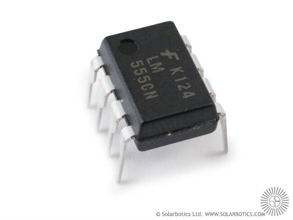
555 timer IC
555 timer IC
One of the most versatile linear ICs is the 555 timer which was first introduced in early 1970 by Signetic Corporation giving the name as SE/NE 555 timer. This IC is a  monolithic timing circuit that can produce accurate and highly stable time delays or oscillation. Like other commonly used op-amps, this IC is also very much reliable, easy to use and cheaper in cost. It has a variety of applications including monostable and astable multivibrators, dc-dc converters, digital logic probes, waveform generators, analog frequency meters and tachometers, temperature measurement and control devices, voltage regulators etc. The timer basically operates in one of the two modes either as a monostable (one-shot) multivibrator or as an astable (free-running) multivibrator.The SE 555 is designed for the operating temperature range from – 55°C to 125° while the NE 555 operates over a temperature range of 0° to 70°C.

The important features of the 555 timer are :

  • It operates from a wide range of power supplies ranging from + 5 Volts to + 18 Volts supply voltage.
  • Sinking or sourcing 200 mA of load current.
  • The external components should be selected properly so that the timing intervals can be made into several minutes Proper selection of only a few external components allows timing intervals of several minutes along with the frequencies exceeding several hundred kilo hertz.
  • It has a high current output; the output can drive TTL.
  • It has a temperature stability of 50 parts per million (ppm) per degree Celsius change in temperature, or equivalently 0.005 %/ °C.
  • The duty cycle of the timer is adjustable with the maximum power dissipation per package is 600 mW and its trigger and reset inputs are logic compatible.

2. IC Pin Configuration

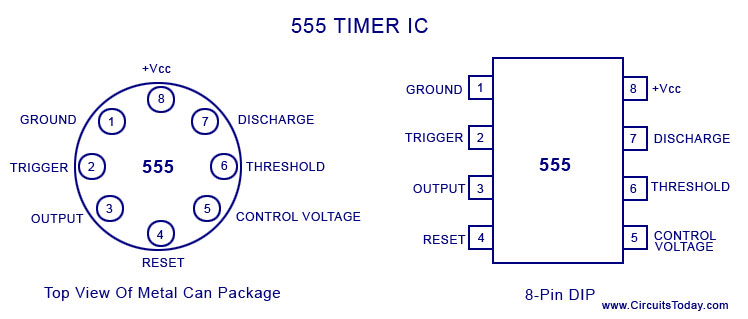
555 timer ic pin configuration and diagram
555 Timer IC Pin Configuration
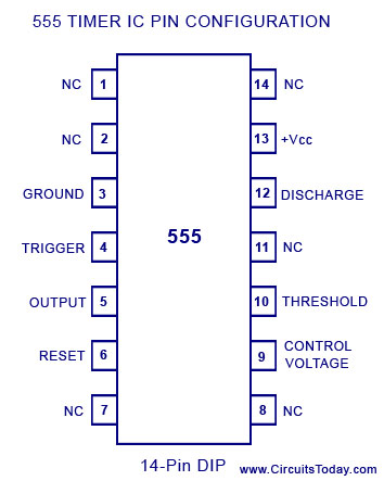
The 555 Timer IC is available as an 8-pin metal can, an 8-pin mini DIP (dual-in-package) or a 14-pin DIP.
This IC consists of 23 transistors, 2 diodes and 16 resistors. The explanation of terminals coming out of the 555 timer IC is as follows. The pin number used in the following discussion refers to the 8-pin DIP and 8-pin metal can packages.
555 timer dual in line package 14 pin configuration

Pin 1: Grounded Terminal: All the voltages are meas­ured with respect to this terminal.
Pin 2: Trigger Terminal: This pin is an inverting input to a comparator that is responsible for transition of flip-flop from set to reset. The output of the timer depends on the amplitude of the external trigger pulse applied to this pin.
Pin 3: Output Terminal: Output of the timer is avail­able at this pin. There are two ways in which a load can be connected to the output terminal either between pin 3 and ground pin (pin 1) or between pin 3 and supply pin (pin 8). The load connected between pin 3 and ground supply pin is called the normally on load and that connected between pin 3 and ground pin is called the normally off load.
Pin 4: Reset Terminal: To disable or reset the timer a negative pulse is applied to this pin due to which it is referred to as reset terminal. When this pin is not to be used for reset purpose, it should be connected to + VCC to avoid any possibility of false triggering.
Pin 5: Control Voltage Terminal: The function of this terminal is to control the threshold and trigger levels. Thus either the external voltage or a pot connected to this pin determines the pulse width of the output waveform. The external voltage applied to this pin can also be used to modulate the output waveform. When this pin is not used, it should be connected to ground through a 0.01 micro Farad to avoid any noise problem.
Pin 6: Threshold Terminal: This is the non-inverting input terminal of comparator 1, which compares the voltage applied to the terminal with a reference voltage of 2/3 VCC. The amplitude of voltage applied to this terminal is responsible for the set state of flip-flop.
Pin 7 : Discharge Terminal: This pin is connected internally to the collector of transistor and mostly a capacitor is connected between this terminal and ground. It is called discharge terminal because when transistor saturates, capacitor discharges through the transistor. When the transistor is cut-off, the capacitor charges at a rate determined by the external resistor and capacitor.
Pin 8: Supply Terminal: A supply voltage of + 5 V to + 18 V is applied to this terminal with respect to ground (pin 1).

3. 555 Timer Basics

The 555 timer combines a relaxation oscillator, two comparators, an R-S flip-flop, and a discharge capacitor.
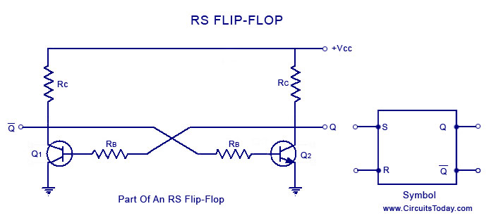
RS Flip Flop in 555 Timer IC
R-S Flip-Flop: – A pair of cross-coupled transistors is shown in figure. Each collector drives the opposite base through resistance RB. In such circuit one transistor is saturated while the other is cut-off. For instance, if transistor Q1 is saturated, its collector voltage is almost zero. So there is no base drive for transistor Q2 and it goes into cut-off and its collector voltage approaches + VCC. This high voltage produces enough base current to keep transistor Q1 in saturation.
On the other hand if transistor Q1 is cut-off, its collector voltage, which is approximately equal to + VCC, drives the transistor Q2 into saturation. The low collector voltage (which is approximately to zero) of this transistor then keeps the transistor Q2 in cut-off.Depending on which transistor is saturated, the Q output is either low or high. By adding more components to the circuit, an R-S flip-flop is obtained. R-S flip-flop is a circuit that can set the Q output to high or reset it low. Incidentally, a complementary (opposite) output Q is available from the collector of the other transistor.
Figure shows the schematic symbol for an R-S flip-flop of any design. The circuit latches in either two states. A high S input sets Q to high; a high R input resets Q to low. Output Q remains in a given state until it is triggered into the opposite state.
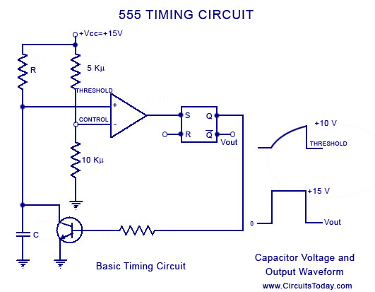
555 Timing Circuit

Basic Timing Concept

Figure illustrates some basic ideas that will prove useful in coming blog posts of the 555 timer. Assuming output Q high, the transistor is saturated and the capacitor voltage is clamped at ground i.e. the capacitor C is shorted and cannot charge.
The non-inverting input voltage of the comparator is referred to as the threshold voltage while the inverting input voltage is referred to as the control voltage. With R-S flip flop set, the saturated transistor holds the threshold voltage at zero. The control voltage, however, is fixed at 2/3 VCC (i.e. at 10 V) because of the voltage divider.
Suppose that a high voltage is applied to the R input. This resets the flip-flop R-Output Q goes low and the transistor is cut-off. Capacitor C is now free to charge. As this capacitor C charges, the threshold voltage rises. Eventually, the threshold voltage becomes slightly greater than (+ 10 V). The output of the comparator then goes high, forcing the R S flip-flop to set. The high Q output saturates the transistor, and this quickly discharges the capacitor. The two waveforms are depicted in figure. An exponential rise is across the capacitor C, and a positive going pulse appears at the output Q. Thus capacitor voltage VC is exponential while the output is rectangular, as illustrated in figure.

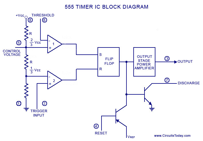
4. Block Diagram


Block Diagram -555 Timer

The block diagram of a 555 timer is shown in the above figure. A 555 timer has two comparators, which are basically 2 op-amps), an R-S flip-flop, two transistors and a resistive network.
  • Resistive network consists of three equal resistors and acts as a voltage divider.
  • Comparator 1 compares threshold voltage with a reference voltage + 2/3 VCC volts.
  • Comparator 2 compares the trigger voltage with a reference voltage + 1/3 VCC volts.
Output of both the comparators is supplied to the flip-flop. Flip-flop assumes its state according to the output of the two compa­rators. One of the two transistors is a discharge transis­tor of which collector is connected to pin 7. This tran­sistor saturates or cuts-off according to the output state of the flip-flop. The saturated transis­tor provides a discharge path to a capacitor con­nected externally. Base of another transistor is connected to a reset terminal. A pulse applied to this terminal resets the whole timer irrespective of any input.

5. Working Principle

Refer Block Diagram of 555 timer IC given above:

Comparator 1 has a threshold input (pin 6) and a control input (pin 5). In most applications, the control input is not used, so that the control voltage equals +2/3 VCC. Output of this comparator is applied to set (S) input of the flip-flop. Whenever the threshold voltage exceeds the control voltage, comparator 1 will set the flip-flop and its output is high. A high output from the flip-flop saturates the discharge transistor and discharge the capacitor connected externally to pin 7. The complementary signal out of the flip-flop goes to pin 3, the output. The output available at pin 3 is low. These conditions will prevail until comparator 2 triggers the flip-flop. Even if the voltage at the threshold input falls below 2/3 VCC, that is comparator 1 cannot cause the flip-flop to change again. It means that the comparator 1 can only force the flip-flop’s output high.
To change the output of flip-flop to low, the voltage at the trigger input must fall below + 1/3 Vcc. When this occurs, comparator 2 triggers the flip-flop, forcing its output low. The low output from the flip-flop turns the discharge transistor off and forces the power amplifier to output a high. These conditions will continue independent of the voltage on the trigger input. Comparator 2 can only cause the flip-flop to output low.
From the above discussion it is concluded that for the having low output from the timer 555, the voltage on the threshold input must exceed the control voltage or + 2/3 VCC. They also turn the discharge transistor on. To force the output from the timer high, the voltage on the trigger input must drop below +1/3 VCC. This also turns the discharge transistor off.
A voltage may be applied to the control input to change the levels at which the switching occurs. When not in use, a 0.01 nano Farad capacitor should be connected between pin 5 and ground to prevent noise coupled onto this pin from causing false triggering.
Connecting the reset (pin 4) to a logic low will place a high on the output of flip-flop. The discharge transistor will go on and the power amplifier will output a low. This condition will continue until reset is taken high. This allows synchronization or resetting of the circuit’s operation. When not in use, reset should be tied to +VCC.

Download 555 Timer Data Sheet:

To know more about NE/SE 555 timer IC check out/download the datasheet. – 

555 Timer as an Astable Multivibrator

An Astable multivibrator, often called a free-running multivibrator,

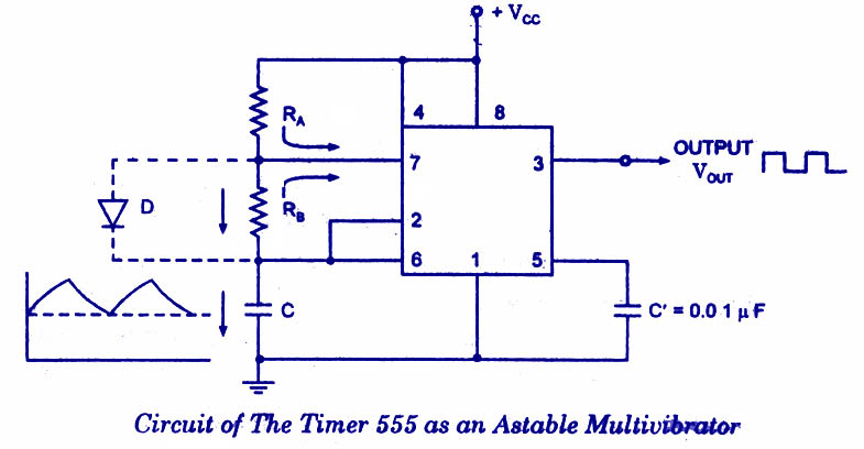
is a rectan­gular-wave generating cir­cuit. Unlike the monostable multivibrator, this circuit does not require any ex­ternal trigger to change the state of the output, hence the name free-running. Before going to make the circuit, make sure your 555 IC is working. For that go through the article: How to test a 555 IC for working An astable multivibrator can be produced by adding resistors and a capacitor to the basic timer IC, as illustrated in figure. The timing during which the output is either high or low is determined by the externally connected two resistors and a capacitor. The details of the astable multivibrator circuit are given below.

555-Astable-Multivibrator
Take a look @ 555 Ic Pin configuration and 555 block diagram before reading further.
Pin 1 is grounded; pins 4 and 8 are shorted and then tied to supply +Vcc, output (VOUT is taken form pin 3; pin 2 and 6 are shorted and the connected to ground through capacitor C, pin 7 is connected to supply + VCC through a resistor RA; and between pin 6 and 7 a resistor RB is connected. At pin 5 either a bypass capacitor of 0.01  F is connected or modulation input is applied.

Astable Multivibrator Operation

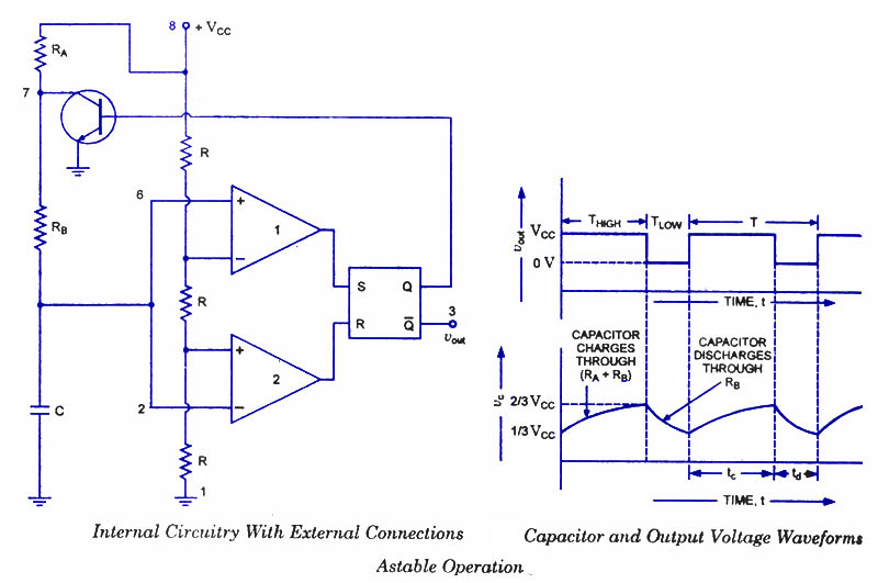
For explaining the operation of the timer 555 as an astable multivibrator, necessary internal circuitry with external connections are shown in figure.

Astable-Multivibrator-Operation
In figure, when Q is low or output VOUT is high, the discharging transistor is cut-­off and the capacitor C begins charging toward VCC through resistances RA and RB. Because of this, the charging time constant is (RA + RB) C. Eventually, the threshold voltage exceeds +2/3 VCC, the comparator 1 has a high output and triggers the flip-flop so that its Q is high and the timer output is low. With Q high, the discharge transistor saturates and pin 7 grounds so that the capacitor C discharges through resistance RB with a discharging time constant RB C. With the discharging of capacitor, trigger voltage at inverting input of comparator 2 decreases. When it drops below 1/3VCC, the output of comparator 2 goes high and this reset the flip-flop so that Q is low and the timer output is high. This proves the auto-transition in output from low to high and then to low as, illustrated in fig ures. Thus the cycle repeats.

Astable Multivibrator using 555 IC -Design method

The time during which the capacitor C charges from 1/3 VCC to 2/3 VCC is equal to the time the output is high and is given as tc or THIGH = 0.693 (RA + RB) C, which is proved below.

Voltage across the capacitor at any instant during charging period is given
as,vc=VCC(1-et/RC)

The time taken by the capacitor to charge from 0 to +1/3 VCC

1/3 VCC = VCC (1-et/RC)

The time taken by the capacitor to charge from 0 to +2/3 VCC

or t2 = RC loge 3 = 1.0986 RC

So the time taken by the capacitor to charge from +1/3 VCC to +2/3 VCC

tc = (t2 – t1) =  (10986 – 0.405) RC = 0.693 RC 

Substituting R = (RA + RB) in above equation we have

THIGH = tc = 0.693 (RA + RB) C

where RA and RB are in ohms and C is in farads.
The time during which the capacitor discharges from +2/3 VCC to +1/3 VCC is equal to
the time the output is low and is given as
td or  TL0W = 0.693 RB C where RB is in ohms and C is in farads The above equation is worked out as follows: Voltage across the capacitor at any instant during discharging period is given as

vc = 2/3 VCC e- td/ RBC

Substituting vc = 1/3 VCC and t = td in above equation we have

+1/3 VCC = +2/3 VCC e- td/ RBC
Or  td = 0.693 RBC

Overall period of oscillations, T = THIGH + TLOW = 0.693 (RA+ 2RB) C , The frequency of oscillations being the reciprocal of the overall period  of oscillations T is given as
f = 1/T = 1.44/ (RA+ 2RB)C
Equation indicates that the frequency of oscillation / is independent of the collector supply voltage +VCC.
Often the term duty cycle is used in conjunction with the astable multivibrator.

The duty cycle, the ratio of the time tc during which the output is high to the total time period T is given as
% duty cycle, D = tc / T * 100 = (RA + RB) / (RA + 2RB) * 100

From the above equation it is obvious that square wave (50 % duty cycle) output can not be obtained unless RA is made zero. However, there is a danger in shorting resistance RA to zero. With RA = 0 ohm, terminal 7 is directly connected to + VCC. During the discharging of capacitor through RB and transistor, an extra current will be supplied to the transistor from VCC through a short between pin 7 and +VCC. It may damage the transistor and hence the timer.

However, a symmetrical square wave can be obtained if a diode is connected across resistor RB, as illustrated in dotted lines in figure. The capacitor C charges through RA and diode D to approximately + 2/3VCC and discharges through resistor RB and terminal 7 (transistor) until the capacitor voltage drops to 1/3 VCC. Then the cycle is repeated. To obtain a square wave output, RA must be a combination of a fixed resistor R and a pot, so that the pot can be adjusted to give the exact square wave.
Although the timer 555 has been used in a wide variety of often unique applications it is very hard on its power supply lines, requiring quite a bit of current, and injecting many noise transients. This noise will often be coupled into adjacent ICs falsely triggering them. The 7555 is a CMOS version of the 555. Its quiescent current requirements are considerably lower than that of 555, and the 7555 does not contaminate the power supply lines. It is pin compatible with the 555. So this CMOS version of the 555 should be the first choice when a 555 timer IC is to be used.

555 Timer as Monostable Multivibrator

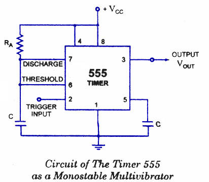
A monostable multivibrator (MMV) often called a one-shot multivibrator, is a pulse generator circuit in which the duration of the pulse is determined by the R-C network,connected externally to the 555 timer. In such a vibrator, one state of output is stable while the other is quasi-stable (unstable). For auto-triggering of output from quasi-stable state to stable state energy is stored by an externally connected capaci­tor C to a reference level. The time taken in storage determines the pulse width. The transition of output from stable state to quasi-stable state is accom­plished by external triggering. The schematic of a 555 timer in monostable mode of operation is shown in figure.
555-timer-monostable-multivibrator
          555-timer-monostable-multivibrator

Monostable Multivibrator Circuit details

Pin 1 is grounded. Trigger input is applied to pin 2. In quiescent condition of output this input is kept at + VCC. To obtain transition of output from stable state to quasi-stable state, a negative-going pulse of narrow width (a width smaller than expected pulse width of output waveform)  and  amplitude of greater than + 2/3 VCC is applied to pin 2. Output is taken from pin 3. Pin 4 is usually connected to + VCC to avoid accidental reset. Pin 5 is grounded through a 0.01 u F capacitor to avoid noise problem. Pin 6 (threshold) is shorted to pin 7. A resistor RA is connected between pins 6 and 8. At pins 7 a discharge capacitor is connected while pin 8 is connected to supply VCC.

555 IC Monostable Multivibrator Operation.


555 monostable-multivibrator-operation
          555 monostable-multivibrator-operation


For explain­ing the operation of timer 555 as a monostable multivibrator, necessary in­ternal circuitry with external connections are shown in figure.

The operation of the circuit is ex­plained below:

Initially, when the output at pin 3 is low i.e. the circuit is in a stable state, the transistor is on and capacitor- C is shorted to ground. When a negative pulse is applied to pin 2, the trigger input falls below +1/3 VCC, the output of comparator goes high which resets the flip-flop and consequently the transistor turns off and the output at pin 3 goes high. This is the transition of the output from stable to quasi-stable state, as shown in figure. As the discharge transistor is cut­off, the capacitor C begins charging toward +VCC through resistance RA with a time constant equal to RAC. When the increasing capacitor voltage becomes slightly greater than +2/3 VCC, the output of comparator 1 goes high, which sets the flip-flop. The transistor goes to saturation, thereby discharging the capacitor C and the output of the timer goes low, as illustrated in figure.

Thus the output returns back to stable state from quasi-stable state.

The output of the Monostable Multivibrator remains low until a trigger pulse is again applied. Then the cycle repeats. Trigger input, output voltage and capacitor voltage waveforms are shown in figure.

Monostable Multivibrator Design Using 555 timer IC

The capacitor C has to charge through resistance RA. The larger the time constant RAC, the longer it takes for the capacitor voltage to reach +2/3VCC.

In other words, the RC time constant controls the width of the output pulse. The time during which the timer output remains high is given as

tp = 1.0986 RAC

where RA is in ohms and C is in farads. The above relation is derived as below. Voltage across the capacitor at any instant during charging period is given as

vc = VCC (1- e-t/RAC)

Substituting vc = 2/3 VCC in above equation we get the time taken by the capacitor to charge from 0 to +2/3VCC.

So +2/3VCC. = VCC. (1 – e-t/RAC)   or   t – RAC loge 3 = 1.0986 RAC
So pulse width, tP = 1.0986 RAC s 1.1 RAC

The pulse width of the circuit may range from micro-seconds to many seconds. This circuit is widely used in industry for many different timing applications.

555 Timer Oscillator

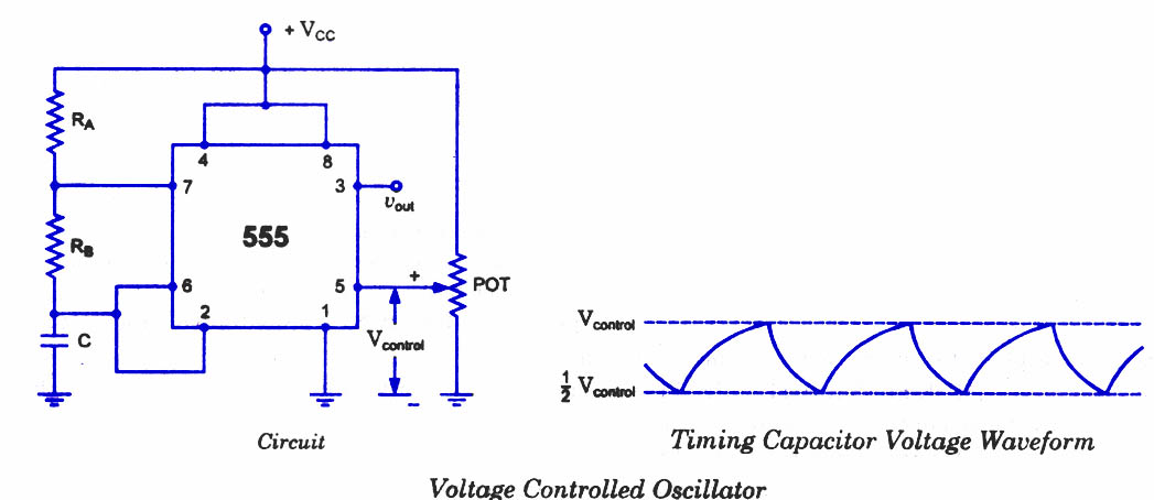
A voltage-controlled oscillator (VCO) using the timer 555 is shown in figure.

555-timer-voltage-controlled-oscillator
             555-timer-voltage-controlled-oscillator

The circuit is sometimes called a voltage-to-frequency converter because the output frequency can be changed by changing the input voltage.
As discussed in previous blog posts, pin 5 terminal is voltage control terminal and its function is  to control the threshold and trigger levels. Normally, the control voltage is ++2/3VCC because of the internal voltage divider. However, an external voltage can be applied to this terminal directly or through a pot, as illustrated in figure, and by adjusting the pot, control voltage can be varied. Voltage across the timing capacitor is depicted in figure, which varies between +Vcontrol and ½ Vcontrol. If control voltage is increased, the capacitor takes a longer to charge and discharge; the frequency, therefore, decreases. Thus the fre­quency can be changed by changing the control volt­age. Incidentally, the control voltage may be made available through a pot, or it may be output of a transistor circuit, op-amp, or some other device

555 Timer-Ramp Generator

Ramp Generator Circuit-using 555 Timer IC

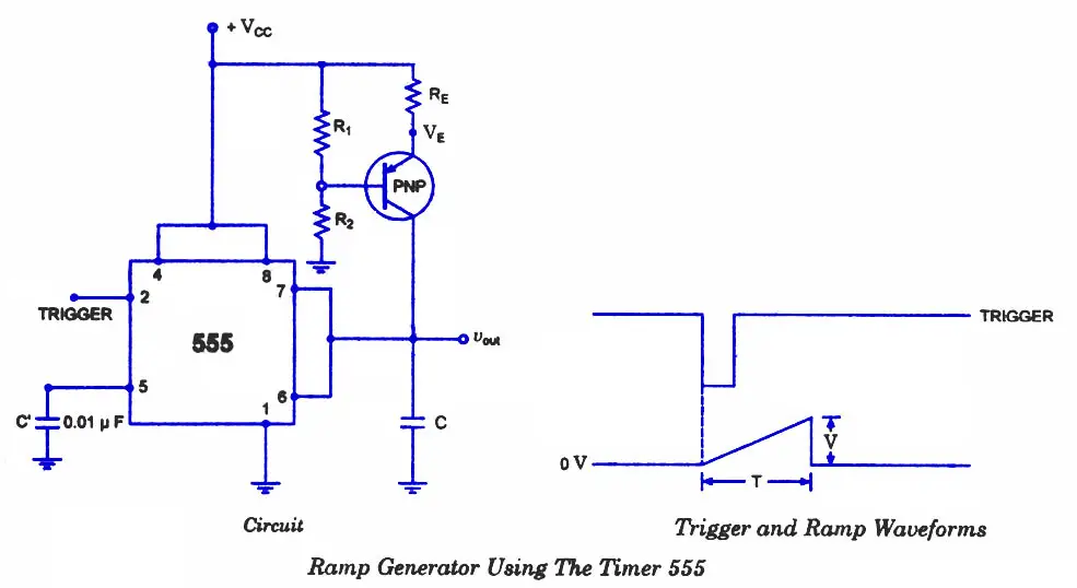
We know that if a capacitor is charged from a voltage source through a resistor, an exponential waveform is produced while charging of a capaci­tor from a constant current source produces a ramp. This is the idea behind the circuit. The circuit of a ramp generator using timer 555 is shown in figure. Here the resistor of previ­ous circuits is replaced by a PNP transistor that produces a constant charging current.

Ramp Generator Circuit
                        Ramp Generator Circuit

Charging current produced by PNP constant current source is

iC = Vcc-VE / RE

where VE = R2 / (R1 + R2) * VCC + VBE
When a trigger starts the monostable multivibrator timer 555 as shown in figure, the PNP current source forces a constant charging into the capacitor C. The voltage across the capacitor is, therefore, a ramp as illustrated in the figure. The slope of the ramp is given as

Slope, s = I/C

Police siren using NE555

Description.

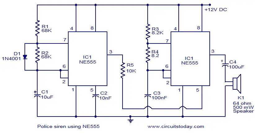
A lot of electronic circuits using NE555 timer IC are already published here and this is just another one.Here is the circuit diagram of a police siren based on NE55 timer IC. The circuit uses two NE555 timers ICs and each of them are wired as astable multivibrators.The circuit can be powered from anything between 6 to 15V DC and is fairly loud.By connecting an additional power amplifier at the output you can further increase the loudness.

IC1 is wired as a slow astable multivibrator operating at around 20Hz @ 50% duty cycle and IC2 is wired as fast astable multivibrator operating at around 600Hz.The output of first astable mutivibrator is connected to the control voltage input (pin5) of IC2. This makes the output of IC2 modulated by the output frequency of IC1, giving a siren effect. In simple words, the output frequency of IC2 is controlled by the output of IC1.

Circuit diagram.
police-siren-using-NE555

Notes.
  • The circuit can be assembled on a Perf board.
  • I used 12V DC for powering the circuit.
  • Instead of using two NE55 timer ICs, you can also use a single NE556 timer.
  • NE556 is nothing but two NE555 ICs in one package.
  • Refer the datasheets of NE555 and NE556 to have a clear idea.
  • Speaker can be a 64ohm, 500mW one.

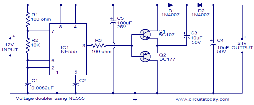
Voltage doubler circuit using NE555

Description.

The circuit diagram of a very simple voltage doubler using NE555 timer is shown here. Here IC NE555 is wired as an astable mutivibrator operating at around 9KHz. The base of the two transistors (Q1 and Q2) is shorted and output of the astable multivibrator (pin 3) is connected to it. When the output of astable multivibrator is low, Q1 will be OFF and Q2 will be ON. The negative terminal of the capacitor C3 will be shorted to ground through T2 and it will be charged to the input supply voltage. When the output of the astable multi vibrator is high, transistor Q1 will be ON and transistor Q2 will be OFF. The capacitor C4 will be charged to the voltage across capacitor C3 plus the input supply voltage (that is double the input voltage). This is how the circuit works.

This voltage doubler circuit can deliver only up to 50mA output current and above that current limit the output voltage will be dramatically reduced. The actual output voltage will be around 19V for a 12V DC input and also the output voltage will be a bit unstable. Anyway, for low current applications this circuit is well enough.

Circuit diagram.
voltage doubler using NE555 timer
  • Notes
  • The circuit can be assembled on a vero board.
  • The output current should not be allowed to exceed 70mA.
  • IC1 must be mounted on a holder.

Page Rank

google pagerank

Write For Us

Submit a Guest Post

Find us on Facebook

Categories

555 Timer IC 7 segment Display 8051 Project AC Circuits Adafruit Alarms Amplifier Circuits Analog Circuits android Arduino arm processor Assembly Languange Atmel Atom Size Audio Circuits augmented reality Automotive Circuits avr Battery Circuits Bicycle Gurad bluetooth Cable TV Circuits Cambridge University Camera Technology Circuit Boards Clipping And Clamping Circuits Clocking And Timer Circuits Computing contact lens Contact Us Form Contests Controller Circuit Conversion Circuits Counter Circuits Digital Electronics diy circuits Downloads EFY EFYTimes Electronic Books Electronic Components Electronic Locks And Keys Engineering Fan Circuits Filter Circuits Fire Alarm free Frequency Fun And Game Circuits future Google Hack n Mod Ham Radio Circuits heart rate monitoring High Voltage Circuits Home Circuits IC Guide ieee Industrial Circuits Infrared Instructables Inventions ipad lcd Led Circuits Light Related Lighting Circuits Medical Circuits Meter Clocks Microcontrollers Microprocessors Mini Projects modules Movie maker NatGeo Navigation Notice Optical Fiber PC Circuits PCB Boards Physics pnp transistor Power Supplies Printing Projects Programmer Project Ideas Projectors Protection circuits Proximity Detectors Radar Radio Circuits Radio Transmitters Raspberry Raspberry Pie Remote Circuits Retis Lab RFID Robot Cars Robotics Science Science Alert Security And Safety Sensor Circuits Servo Motors Smallest Smartwatches sms Software solar cell sound application Spectram Switch Technology News Telephone Related Television Related Test And Measurement Circuits Thermal Projects Tone generator circuits Touch Screen Tutorials Wearables Wi-Fi Wireless
Like us on Facebook
Follow us on Twitter
Recommend us on Google Plus
Subscribe me on RSS