Search This Blog

Powered by Blogger.

Translate

Cascode amplifier

Cascode amplifier is a two stage circuit consisting of a transconductance amplifier followed by a buffer amplifier. The word “cascode” was originated from the phrase “cascade to cathode”. This circuit have a lot of advantages over the single stage amplifier like, better  input output isolation, better gain, improved bandwidth, higher input impedance, higher output impedance, better stability, higher slew rate etc. The reason behind the increase in bandwidth is the reduction of Miller effect.  Cascode amplifier is generally constructed using FET ( field effect transistor) or BJT ( bipolar junction transistor). One stage will be usually wired in common source/common emitter mode and the other stage will be wired in common base/ common emitter mode.

Miller effect.

Miller effect is actually the multiplication of the drain to source stray capacitance by the voltage gain. The drain to source stray capacitance always reduces the bandwidth and when it gets multiplied by the voltage gain the situation is made further worse. Mulitiplication of stray capacitance increases the effective input capacitance and as we know, for an amplifier, the increase in input capacitance increases the lower cut of frequency and that means reduced bandwidth. Miller effect can be reduced by adding a current buffer stage at the output of the amplifier or by adding a voltage buffer stage before the input.

FET Cascode amplifier.
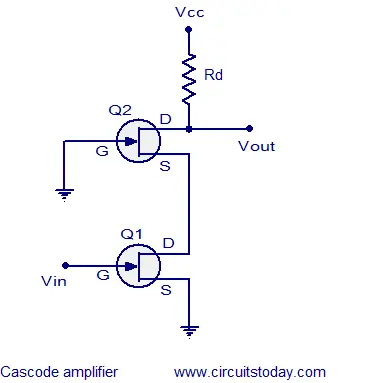

FET cascode amplifier
The circuit diagram of a typical Cascode amplifier using FET is shown above. The input stage of the circuit is an FET common source amplifier and the input voltage (Vin) is applied to its gate. The output stage is an FET common gate amplifier which is driven by the input stage. Rd is the drain resistance of the output stage. Output voltage (Vout)  is taken from the drain terminal of Q2. Since the gate of Q2 is grounded, FET Q2′s source voltage and the FET Q1′s drain voltage are held almost constant. That means the upper FET Q2 offers a low input resistance to the lower FET Q1. This reduces the gain of lower FET Q1 and as a result the Miller effect also gets reduced which results in increased bandwidth. The reduction in gain of the lower FET Q1 does not affect the overall gain because the upper FET Q2 compensates it. The upper FET Q2  is not affected by the Miller effect because the charging and discharging of the drain to source stray capacitance is carried out through the drain resistor and the load and the frequency response if affected only for high frequencies (well over the audio range).
In Cascode configuration, the output is well isolated from the input. Q1 has almost constant voltage at the drain and source terminals while Q2 has almost constant voltage at its source and gate terminals and practically there is nothing to feed back from the output to input. The only points with importance in terms of voltage are the input and output terminals and they are well isolated by a central connection of constant voltage.

Practical Cascode amplifier circuit.
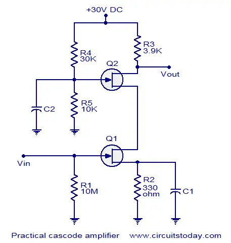
FET cascode amplifier
Practical cascode amplifier circuit
A practical Cascode amplifier circuit based on FET is shown above. Resistors R4 and R5 form a voltage divider biasing network for the FET Q2. R3 is the drain resistor for Q2 and it limits the drain current. R2 is the source resistor of Q1 and C1 is its by-pass capacitor. R1 ensures zero voltage at the gate of Q1 during zero signal condition


source:circuitstoday.com

Google Project Glass : Way To New Evolution

Google (Nasdaq: GOOG) has revealed its long-rumored plans to create augmented reality (AR) eyeglasses.
Google's Project Glass
Augmented reality is a live, direct or indirect view of a physical environment that's augmented by computer-generated input such as sound, video, graphics or GPS data.
Work on the AR glasses is proceeding as Project Glass, which is part of the Google X Lab, a facility run by Google said to be somewhere in California's Bay Area where about 100 leading-edge projects are reportedly being undertaken.
The scientists behind Project Glass are Babak Parviz, Steve Lee and Sebastian Thrun. They asked for viewer feedback on a video they posted on YouTube.
Through the Looking Glass
The video is shot from the point of view of someone wearing a pair of AR glasses. The wearer can apparently take a phone call while wearing the glasses, listening and speaking with the caller, whose avatar or photo pops up on one lens of the glasses.
 
 
The wearer can also transmit what he or she sees during the conversation. For example, looking out of the window triggers data about the weather that's shown on the lens.
Looking at objects while walking pulls up information on the lens. For example, when the wearer passes a subway station, a notice that service had been suspended is called up a Google Map showing a walking route.
A Siri-like voice application puts up information in response to questions. For example, when the user walked into a bookstore and asked where the music section was, a map indicating that section came up on the lens.
The user can also instruct the glasses to take a photo.
Project Glass seems to incorporate features from Google Maps, Android's voice response system, Google's geolocation service and other features.
"We plan to share a lot more details as we continue to work on this project," Google spokesperson Katelin Todhunter-Gerberg told TechNewsWorld. However, "our only on-the-record statement is in the Google+ post." 


Who's Making the Glasses

Babak Parviz, from the Project Glass Team, is an associate professor of electrical engineering at the University of Washington who has been working on bionic contact lenses that could wirelessly stream information across their surface, much like the AR glasses.
He led a team that created a prototype contact lens that contained a single pixel of information as a proof of concept. The lens has an antenna to draw power from an external source. An integrated circuit in the lens stores this energy and transfers it to a transparent sapphire chip containing one blue LED.
Another member of the Project Glass team, Sebastian Thrun, is a Google Fellow and a part-time research professor of computer science at Stanford University. He was formerly the director of the Stanford Artificial Intelligence Laboratory and led the development of the Google self-driving car.

My AR Glasses Cup Runneth Over

"The question is whether [AR glasses] will initially be more helpful or more annoying," Rob Enderle, principal analyst at the Enderle Group, told TechNewsWorld.
"Let's say you are driving, and just before the guy in front of you hits his brakes a note pops up warning you of traffic ahead so you don't actually see his brake lights in time," he said. "In that instance, the glasses will become a huge liability."
However, if the glasses work, Enderle will use them. "They would alert me to things I want to know and likely otherwise would miss," he explained. "And they'd be very handy in navigation, particularly while walking or on a bike."
Google will have to work out some knots in its idea first in order to have the glasses accepted by the general public.
"Putting something over someone's eyes to create a new human/machine interface is fascinating, but given how much we use our eyes, it doesn't come without risk," Enderle pointed out.
"This is like the 3D TV thing all over again," Maribel Lopez, principal analyst at Lopez Research, told TechNewsWorld. "Nobody wants to buy 3D TV because nobody wants to wear the dorky glasses."
Further, it's not likely that people whose vision doesn't require correcting would want to wear AR glasses, Lopez pointed out. "It's got to be something that's integrated into your normal routine, like cycling glasses for when you're going to ride your bike, and not a stretch." 
 
 
Source:http://www.technewsworld.com/rsstory/74784.html

Microcontroller Based Water Level Control System


The present concept implements controlling of pump which pumps water from the sump (underground tank) to the overhead tank, using 8951 microcontroller.
The control panel, i.e. the main control unit of the system which consists of the primary control switches, pump indicator, siren and level indicators. The visual example of how switches And the indicators can be placed as shown the figure below.
Front view of the model
In the figure shown above there are total of nine LEDs, four of which indicates the water level in the tank, another four indicates the water level in the sump and one LED indicates whether the pump is ON/OFF. It also consists of three switches.
  1. Switch 1 is the main power switch which is used to activate the system.
  2. Switch 2 is used to select whether to operate the pump in AUTO or MANUAL mode.
  3. Switch 3 comes to picture only when the system is operated in MANUAL mode. It controls the direct activation of the pump.
Description :
This system is built around an 8951 microcontroller and the circuit diagram is as given below.
Circuit diagram of Water level indicator cum controller
As you can see in the above diagram, port 0 is exclusively used as an input port which takes the information regarding the water level in the sump as well as in the overhead tank.
Port 1 is used as output port which is connected to the indicator that indicates the water level in both the tanks.
Port 2 is used as in/out port, it takes the input from switch 2 and switch 3 and gives the output which is connected to pump indicator, siren and the relay which controls the switching of the pump.
Working of the system:
There are two modes of working for the system
  1. Manual mode
  2. Auto mode
Which is controlled by switch 2 (refer control panel diagram)
Manual mode:
When the system is active and in manual mode, it only indicates the water levels in the tanks and it doesn’t control any working of the pump. To activate the pump in manual mode switch 3 is used.
In this mode the operator should manually control the working of the pump. As in case  if the tank is full, operator should switch of the pump which is not the case when compared to auto mode.
Auto mode:
When the system is active and in auto mode, it only indicates the water levels in the tanks and it controls the working of the pump.


Programm:


;********************************************************************************************
;Objective : Water Level Indicater and Motor Protection
;Name of the Programmer : Prateek Kaura
;Hardware Used : CPU Board, Led Card, Power Supply, 8 pin connector
; Two pin connector
;Program Description ; Crystal=11.0592kHz
; Port0 is used as LCD
; Port1 is used for Motor
; Port2 is used for LED’s
; Port3 is used for RF Module
;Status :
;**********************Hardware declaration**************************************************;
lcd equ p0
RS BIT P2.5
EN BIT P2.4
buzzer bit p2.3
GREEN bit p2.0
YELLOW bit p2.1
RED bit p2.2
senser1 bit p3.0
senser2 bit p3.1
senser3 bit p3.2
senser4 bit p3.3
relay1 bit p1.0
key1 bit p1.3
;*********************************************************************************************;
ORG 0000H ;RESET OPERATION
SJMP POWERON ;GO TO POWERON LABEL
ORG 0003H ;EXTERNAL0 INTERRUPT
RETI ;RETURN FROM THE INTERRUPT
ORG 000BH ;TIMER0 INTERRUT
RETI ;RETURN FROM THE INTERRUPT
ORG 0013H ;EXTERNAL1 INTERRUPT
RETI ;RETURN FROM THE INTERRUPT
ORG 001BH ;TIMER1 INTERRUPT
; ljmp timer1
RETI ;RETURN FROM THE INTERRUPT
ORG 0023H ;SERIAL COMMUNICATION INTERRUPT
RETI ;RETURN FROM THE INTERRUPT
ORG 0030H
POWERON: MOV SP,#70H ; Move the stack pointer at 70h location
MOV IE,#00H ; Disable all the interrupts
MOV IP,#00H ; Disable the interrupt priority register
MOV P0,#0FFH ; Move 0FFH in in port 0
MOV P1,#0FFH ; Move 0FFH in in port 1
MOV P2,#0FFH ; Move 0FFH in in port 2
MOV P3,#0FFH ; Move 0FFH in in port 3
;*RAM variable declaration ,30h-7Fh
;……………………………………….
;……………………………………….
;*********************************************************************************************;
;*****************POWER ON *************************************************************** ;
;****************************RAM CLEARANCE**********************************************;
MOV R0,#7FH
RAM_CLR: MOV @R0,#00H ; Clear the RAM from 00 to 7FH
DJNZ R0,RAM_CLR
;;**********************************MAIN PROG******************************************************
setb red
setb yellow
setb green
clr relay1
mov lcd,#38h
acall command
mov lcd,#01h
acall command
mov lcd,#0eh
acall command
mov lcd,#80h
acall command
MOV DPTR,#DATA1
ACALL DISPLAY_
main1:
setb red
setb yellow
setb green
mov r2,#70d
main3:
setb green
setb RELAY1
acall delay
jnb senser1,check1
djnz r2,main3
mov r2,#50d
sjmp main5
main11:
jnb p1.3,main3
sjmp main11
main:
setb buzzer
setb green
setb red
setb yellow
jnb senser1,check1
sjmp main
main5:
clr relay1
acall delay
setb green
setb red
setb yellow
mov lcd,#0c0h
acall command
MOV DPTR,#level4
ACALL DISPLAY_
acall command
sjmp main11
check1:
clr green
setb red
setb YELLOW
jb senser1,main3
jnb senser2,check2
mov lcd,#0c0h
acall command
MOV DPTR,#level1
ACALL DISPLAY_
djnz r2,check1
mov r2,#20
sjmp main
check2:
clr YELLOW
clr green
setb red
;jnb p3.2,main3
jnb senser3,check3
jb senser2,main
mov lcd,#0c0h
acall command
MOV DPTR,#level2
ACALL DISPLAY_
sjmp check2
check3:
clr red
mov r3,#04
clr YELLOW
clr green
clr relay1
buzzer_on:
clr buzzer
acall delay
setb buzzer
acall delay
jb senser3,main
mov lcd,#0c0h
acall command
MOV DPTR,#level3
ACALL DISPLAY_
djnz r3,buzzer_on
check34:
setb buzzer
acall delay
clr red
clr YELLOW
clr green
clr relay1
jb senser3,main7
mov lcd,#0c0h
acall command
MOV DPTR,#level3
ACALL DISPLAY_
sjmp check34
main7:
ljmp main
DISPLAY_:
CLR A
MOVC A,@A+DPTR
MOV LCD,A
ACALL DATA
INC DPTR
JZ EXIT
SJMP DISPLAY_
EXIT:
RET
;****************command*************
command:
clr RS
setb EN
nop
nop
nop
nop
nop
clr EN
ACALL DELAY
ret
;*****************data***************
data:
setb RS
setb EN
nop
nop
nop
nop
nop
clr EN
ACALL DELAY
ret
;***************************delay***************************************
delay:
mov 33h,#50d
loop1: mov 34h,#50d
loop2: mov 35h,#20d
loop3: djnz 35h,loop3
djnz 34h,loop2
djnz 33h,loop1
ret
;**************************************data byte******************************************************************
ORG 300H
DATA1:
DB ‘ WATER LEVEL ‘,0
level1:
DB ‘Low Level ‘,0
level2:
DB ‘Medium Level ‘,0
level3:
DB ‘High Level ‘,0
level4:
DB ‘Input Line Fail ‘,0


Pyroelectric Fire Alarm System


This is definitely an ultra-sensitive fire sensor that exploits the direct piezoelectric property of an ordinary piezo component to recognize the fire. The lead zirconate titanate crystals within the piezo component have the property to deform and produce an electrical potential when heated, thus converting the piezo component into a heat sensor. The circuit mentioned right here is really sensitive. It provides a warning alarm in the event the area temperature raises over 10°C. The whole circuit has two modules: the sensor module and also the power supply module.

The Sensor circuit
The front end of the circuit contains a sensitive signal amplifier constructed close to IC1 (CA3130). It delivers a high output when temperature near the piezo component raises. IC CA3130 is really a CMOS operational amplifier with gate protected p-channel MOSFETs inside the inputs. It has high speed of operation and low input current specifications. There are certainly two inputs-the non-inverting input (pin 3) connected to the piezo component via diode D7 (OA71) that carries the voltage signal from the piezo component and the inverting input (pin 2) that gets a preset voltage through VR1.
By adjusting VR1, it is very easy to set the reference voltage level at pin 2. In normal condition, IC1 provides a low output and the remaining circuitry is within a standby state. Capacitor C2 keeps the non-inverting input of IC1 stable, so that even a slight change in voltage level in the inputs can change the output to high.
Typically, IC1 provides a low output, trying to keep transistor T1 non-conducting. Reseting pin 12 of IC2 (CD4060) connected to the collector of transistor T1 gets a high voltage via R5 and IC2 stays disabled. Once the piezo component gets heat from fire, asymmetry in its crystals causes a potential change, enabling capacitor C2 to discharge. It momentarily modifies the voltage level at pin 3 of IC1 and its output swings high. Transistor T1 conducts taking the reset pin 12 of IC2 to ground. IC2 is now enabled and gets going oscillating. With the shown values of the oscillating parts C3 (0.22µ) and R6 (1M), the first output (Q3) turns high right after several seconds along with a red LED2 starts flashing. If heat near the piezo persists, Q7 (pin 14) output of IC2 becomes high after one minute, and also the alarm will start beeping. If heat continues, Q9 (pin 15) turns high after 4 minutes and turns on the relay driver transistor T2. Simultaneously, diode D8 conducts and IC2 stops oscillating and toggles.
The solenoid pump connected to the N/O (normally opened) contact of the relay starts spraying the fire-ceasing foam or water to the probable sites of fire.
The power supply circuit
Pyroelectric Fire Alarm System circuit
Power supply comprises a 0-12V, 1A step-down transformer having a standard full-wave rectifier formed by D1 through D4 and filter capacitor C1. A battery backup is supplied when the mains supply is cut-off because of short-circuit and fire. A 12V, 4.5Ah rechargeable battery is utilized for backup to provide enough current for the solenoid pump. When mains electrical power is available, diode D5 forward biases. It provides power towards the circuit and also charges the battery via resistor R2, and it limits the charging current to 120 mA. When power fails, diode D5 reverse biases and diode D6 forward biases, providing immediate backup for the circuit. LED1 signifies the availability of mains electrical power.
Assemble the circuit on a general purpose PCB and enclose it inside a appropriate case. Connect the piezo component to the circuit by using a thin insulated wire. Glue the flat side of the piezo component on a 30×30cm aluminium sheet to improve its sensitivity. Work on the sheet with the piezo sensor to the site in which protection is necessary. The remaining circuit could be fixed at a proper spot. If only the alarm generator is required, omit the relay driver section.
Download the circuit and explanation in PDF file: Pyroelectric Fire Alarm System

Mini UPS


Here the simple Mini UPS circuit diagram. This circuit can provide an uninterrupted power supply (UPS) to operate 12V, 9V and 5V DC-powered instruments at up to 1A current. The backup battery will take up the load with no spikes or delay when the mains electrical power gets interrupted. It could possibly also be utilized as a workbench power supply that delivers 12V, 9V and 5V operating voltages. The circuit instantly disconnects the load when the battery voltage decreases to 10.5V to avoid deep discharge of your battery. LED1 indication is presented to indicate the complete charge voltage level of the battery. Miniature white LEDs (LED2 and LED3) are utilized as emergency lamps especially during electrical power failure at night time.
A common step-down transformer delivers 12V of AC, that is rectified by diodes D1 and D2. Capacitor C1 features ripple-free DC to charge the battery and to the remaining circuit. When the mains electrical power is on, diode D3 gets forward biased to charge the battery. Resistor R1 limits the charging current. Potentiometer VR1 (10k) with transistor T1 acts as being the voltage comparator to indicate the voltage level. VR1 is so adjusted that LED1 is in the ‘off’ mode. when the battery is completely charged, LED1 glows indicating a maximum voltage level of 12V.
Download the circuit diagram of Mini UPS and full explanation about how it’s work, download this PDF file:
» Download Link

Low Cost Water Pump Controller circuit


Here the circuit diagram of low cost water pump controller. The automatic pump controller minimizes the need for any manual switching of water pumps installed for the functionality of pumping water from a reservoir to an overhead tank . It instantly switches on the pump once the water level within the tank falls below a specific low level (L), provided the water level in the reservoir is above a specific level (R). Subsequently, because the water level in the tank increases to an upper level (M), the pump is turned off instantly. The pump is turned on again only if the water level once again falls beneath level L in the tank, provided the level inside the reservoir is above R. This automated action
continues.


The circuit is intended to ‘overlook’ the transient oscillations of the water level that would otherwise trigger the logic to modify its state rapidly and unnecessarily. The circuit works by using a single CMOS chip (CD4001) for logic processing.
No utilization of any moving electromechanical elements within the water-level sensor has been made. This assures fast reaction, no wear and tear, and no mechanical problems. The circuit diagram can be seen on above image. The unit performed satisfactorily on a test run in conjunction with a 0.5 HP motor and pump.
The sensors applied to the circuit could be any two conducting probes, preferably resistant to electrolytic corrosion. For example, in the easiest case, a appropriately sealed audio jack could be utilized to operate as the sensor.
Low Cost Water Pump Controller circuit
The circuit may also be utilized like a constant fluid level maintainer. For this objective, the probes M and L are brought pretty near to one another to make sure that the fluid level is maintained within the M and L levels.
The benefit of this system is that it could be applied to tanks/reservoirs of any volume whatsoever. Even so, the circuit can’t be applied for purely non-conducting fluids. For non-conducting fluids, some modifications have to be prepared in the fluidlevel sensors. The circuit can on the other hand be kept intact.

Motion Sensor Light Switch


Motion Sensor Light Switch Circuit

Today many available commercial motion sensor light switches on the market, one of the brands that are sought after a Leviton motion sensor light switch type PR180-1LW Leviton decora Incandescent 500W, Passive Infrared Wall Switch Occupancy Sensor. You can buy it at a price of about $ 15. Motion sensors are widely used for home security, office, or the places that require extra security.
Motion sensor light switch is a human motion detector that works in a range of infrared detection. If the PIR sensor devices receive the infrared energy emitted by the human body, it will eventually be switching relay which in turn will turn on the lights. So the function of the use of this switch sensor for security purposes, particularly at nighttime conditions.
In addition to buying a human motion detector, if you want to do it yourself (DIY), a motion sensor switch, is now also widely available PIR sensor modules that are sold in general, so that by adding a high-gain amplifier which is equipped with a relay switch, then this it works as a motion sensor light switch.

Motion Sensor Light Switch Circuit Diagram

Here is a motion sensor light switch circuit is quite simple using the SB0061, the pyroelectric sensor module, developed to detect human body. A PIR detector combined with a Fresnel lens mounted on a compact with analog IC card (SB0061) and a limited part of the module. High-level output (3.3) pre-adjustable variable width (5secs -18 minutes) is provided.

PIR Motion Sensor Light Switch Circuit
PIR motion sensor light switch schematic on SB0061 presented here can be used for a security lighting or energy saving mode corridor. 12V DC required for the entire circuit can be powered by standard 12V AC adapter / battery.

Motion Sensor Light Switch Circuit – How It Works

Development of a simple motion sensor circuit and easy. When motion is detected at about 5-6 meters, or about 3.3 volts appears at the base of the transistor T1 and T2 to participate in the next relay driver transistor light. Therefore, the relay DPDT 12V to power the white LED current limit resistor R3. Spare relay contacts can be used as a switch controlling the external load correctly. White LED and relay will remain for a period of time depending on mono SB0061, 5 seconds to 18 minutes. Source: Motion Sensor Light Switch

Page Rank

google pagerank

Write For Us

Submit a Guest Post

Find us on Facebook

Categories

555 Timer IC 7 segment Display 8051 Project AC Circuits Adafruit Alarms Amplifier Circuits Analog Circuits android Arduino arm processor Assembly Languange Atmel Atom Size Audio Circuits augmented reality Automotive Circuits avr Battery Circuits Bicycle Gurad bluetooth Cable TV Circuits Cambridge University Camera Technology Circuit Boards Clipping And Clamping Circuits Clocking And Timer Circuits Computing contact lens Contact Us Form Contests Controller Circuit Conversion Circuits Counter Circuits Digital Electronics diy circuits Downloads EFY EFYTimes Electronic Books Electronic Components Electronic Locks And Keys Engineering Fan Circuits Filter Circuits Fire Alarm free Frequency Fun And Game Circuits future Google Hack n Mod Ham Radio Circuits heart rate monitoring High Voltage Circuits Home Circuits IC Guide ieee Industrial Circuits Infrared Instructables Inventions ipad lcd Led Circuits Light Related Lighting Circuits Medical Circuits Meter Clocks Microcontrollers Microprocessors Mini Projects modules Movie maker NatGeo Navigation Notice Optical Fiber PC Circuits PCB Boards Physics pnp transistor Power Supplies Printing Projects Programmer Project Ideas Projectors Protection circuits Proximity Detectors Radar Radio Circuits Radio Transmitters Raspberry Raspberry Pie Remote Circuits Retis Lab RFID Robot Cars Robotics Science Science Alert Security And Safety Sensor Circuits Servo Motors Smallest Smartwatches sms Software solar cell sound application Spectram Switch Technology News Telephone Related Television Related Test And Measurement Circuits Thermal Projects Tone generator circuits Touch Screen Tutorials Wearables Wi-Fi Wireless
Like us on Facebook
Follow us on Twitter
Recommend us on Google Plus
Subscribe me on RSS