
Labels:
Contact Us Form
Low cost fire alarm circuit
Description.
When there is a fire breakout in the room the temperature increases.This ultra compact and low cost fire alarm senses fire breakout based on this fact.
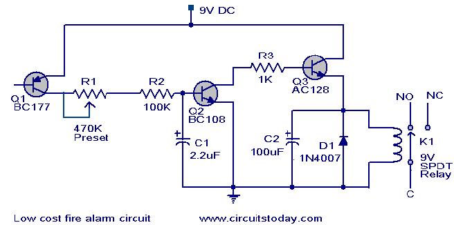
Transistor BC177 (Q1) is used as the fire sensor here.When the temperature increases the leakage current of this transistor also increases.The circuit is designed so that when there is an increase in the leakage current of Q1 ,transistor Q2 will get biased.As a result when there is a fire breakout the transistor Q2 will be on.The emitter of Q2 (BC 108)is connected to the base of Q3(AC 128).So when Q2 is ON Q3 will be also ON.The transistor Q3 drives the relay which is used to drive the load ie,light,bell,horn etc as an indication of the fire.The diode D1 is used as a free wheeling diode to protect it from back EMF generated when relay is switched.
Circuit diagram with Parts list.
Notes.
- The Preset R1 can be used to desired temperature level for setting the alarm ON.
- This is not a latching alarm,ie;when the temperature in the vicinity of the sensor decreases below the set point the alarm stops.
- The circuit can be powered using a 9V battery or a 9V battery eliminator.
- All capacitors are electrolytic and must be rated at least 10V.
- The load can be connected through the C,NC,NO points of the relay according to your need.
- The calibration can be done using a soldering iron,and a thermo meter.Switch ON the power supply.Keep the tip of soldering iron near to the Q1.Same time also keep the thermometer close to it.When the temperature reaches your desired value adjust R1 so that relay gets ON.Done
Fire alarm circuit
Description.
Here is a simple fire alarm circuit based on a LDR and lamp pair for sensing the fire.The alarm works by sensing the smoke produced during fire.The circuit produces an audible alarm when the fire breaks out with smoke.
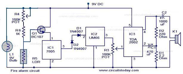
When there is no smoke the light from the bulb will be directly falling on the LDR.The LDR resistance will be low and so the voltage across it (below .6V).The transistor will be OFF and nothing happens.When there is sufficient smoke to mask the light from falling on LDR, the LDR resistance increases and so do the voltage across it.Now the transistor will switch to ON.This gives power to the IC1 and it outputs 5V.This powers the tone generator IC UM66 (IC2) to play a music.This music will be amplified by IC3 (TDA 2002) to drive the speaker.Resistor R6 is meant for protecting the transistor when R4 is turned towards low resistance values .Resistor R2 and R1 forms a feedback network for the TDA2002 and C1 couples the feed back signal from the junction of R1 & R2 to the inverting input of the same IC.
The diode D1 and D2 in combination drops 1.4 V to give the rated voltage (3.5V ) to UM66 .UM 66 cannot withstand more than 4V.
Circuit diagram with Parts list.
Fire alarm circuit
Notes.
- The speaker can be a 32Ω tweeter.
- POT R4 can be used to adjust the sensitivity of the alarm.
- POT R3 can be used for varying the volume of the alarm.
- Any general purpose NPN transistor(like BC548,BC148,2N222) can be used for Q1.
- The circuit can be powered from a 9V battery or a 9V DC power supply.
- Instead of bulb you can use a bright LED with a 1K resistor series to it.
Power supply for the circuit.
A well regulated power supply is essential for this circuit because even slight variations in the supply voltage could alter the biasing of the transistor used in the fire sensing section and this could seriously affect the circuit’s performance.
9V/500mA power supply circuit
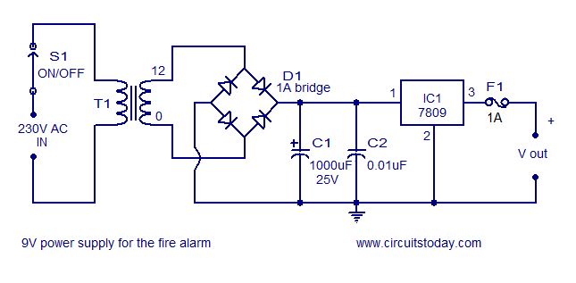
A regulated 9V/500mA power supply that can be used for powering the basic fire alarm circuit and its modified versions is shown above. Transformer T1 is a 230V primary, 12V secondary, 500mA step down transformer. D1 is a 1A bridge which performs the job of rectification. Capacitor C1 filters the rectifier output and C2 is the AC by-pass capacitor. IC1 (7809) is a 9V fixed positive voltage regulator. The output of the rectifier+filter section is connected to the input of 7805 and a regulated steady 9V is obtained at its output. S1 is the ON/OFF switch. F1 is a 500mA safety fuse.
Relay version of the circuit.
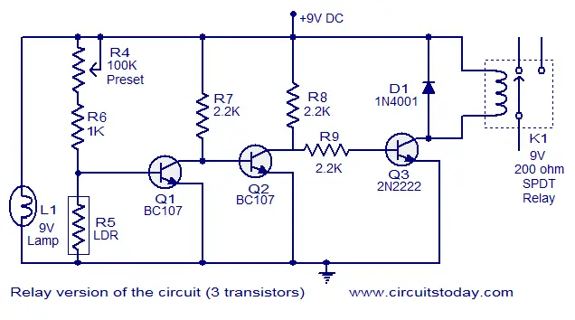
Here the above fire alarm circuit is modified to operate a relay when the fire breaks out. The usage of relay makes the circuit able to switch high power warning devices like alarms, bells,beacon lights etc that operates from the mains.
Relay version of the circuit
Two additional transistors are used with the basic fire sensing circuitry (consisting of Q1, R4, R5 and L1) to attain the target. Whenever the fire breaks out the transistor Q1 is switched ON. The collector voltage of Q1 drops to 0.2V and the transistor Q2 gets switched OFF. This makes the collector voltage of Q2 rise towards 9V and this result in the switching ON of transistor Q3. The relay connected at the collector of Q3 is activated and the load connected through the relay contact is driven. Resistors R7 and R8 limits the collector current of Q1 and Q2 respectively. D1 is a freewheeling diode which protects Q3 from the voltage spikes induced when the relay is switched. Resistor R9 controls the base current of transistor Q3 (2N2222)
Labels:
Fire Alarm,
Security And Safety
Fire alarm using thermistor & NE555
Description.
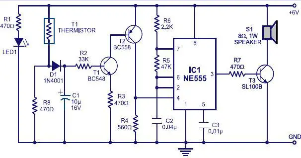
Many fire alarm circuits are presented here,but this time a new circuit using a thermistor and a timer to do the trick. The circuit is as simple and straight forward so that , it can be easily implemented.The thermistor offers a low resistance at high temperature and high resistance at low temperature. This phenomenon is employed here for sensing the fire.
The IC1 (NE555) is configured as a free running oscillator at audio frequency. The transistors T1 and T2 drive IC1. The output(pin 3) of IC1 is couples to base of transistor T3(SL100), which drives the speaker to generate alarm sound. The frequency of NE555 depends on the values of resistances R5 and R6 and capacitance C2.When thermistor becomes hot, it gives a low-resistance path for the positive voltage to the base of transistor T1 through diode D1 and resistance R2. Capacitor C1 charges up to the positive supply voltage and increases the the time for which the alarm is ON. The larger the value of C1, the larger the positive bias applied to the base of transistor T1 (BC548). As the collector of T1 is coupled to the base of transistor T2, the transistor T2 provides a positive voltage to pin 4 (reset) of IC1 (NE555). Resistor R4 is selected s0 that NE555 keeps inactive in the absence of the positive voltage. Diode D1 stops discharging of capacitor C1 when the thermistor is in connection with the positive supply voltage cools out and provides a high resistance path. It also inhibits the forward biasing of transistor T1.
Circuit diagram with Parts list.
Notes.
- The circuit can be powered from a 6V battery or a 6V power supply
- The thermistor can be mounted on a heat resistant material like mica to prevent it from damage due to excessive heat.
- The LED acts as an indication when the power supply is switched ON
Labels:
Fire Alarm
Filter Circuits

Filter-circuit
The output from any of the rectifier circuit is not purely dc but also has some ac components called ripples, along it. The ripples are maximum in the single phase half-wave rectifier and being reduced in the full-wave rectifier and being reduced further with the increase in the number of phases.
Such supply is not useful for driving sophisticated electronic devices/circuits. Of course, for a circuit such as battery charger the pulsating nature of supply available from a rectifier is no great detriment as long as the dc level provided results in charging of battery. But for supply circuits to radio or tape-recorder the pulsating dc results in 50 – (or 100) Hz signal appearing in the output, thereby making the operation of the overall circuit poor. For such applications, as well as for many more, the output dc developed will have to be much steady or smoother than that of the pulsating dc obtained directly from half-wave or full-wave rectifier circuits.
Hence, it becomes essential to reduce the ripples from the pulsating dc supply available from rectifier circuits to the minimum. This is achieved by using a filter or smoothing circuit which removes (or filters out) the ac components and allows only the dc component to reach the load. Obviously, a filter circuit should be placed between, the rectifier and the load, as shown in figure.
A filter circuit is a device that converts pulsating output of a rectifier into a steady dc level.
A filter is generally a combination of inductors L and Capacitors C. The filtering action of L and C depends upon the facts that an inductor allows only dc and a capacitor allows ac only to pass. So a suitable L and C network can effectively filter out (or remove) the ac components from the rectified output.
Commonly used types of filter circuits are:
(a) Series Inductor filter
(b) Shunt Capacitor Filter
(c) Choke Input Filter
(d) Capacitor input or pie filter
(e) R-C filter
Labels:
Filter Circuits,
Tutorials
Shunt capacitor filter
Shunt Capacitor Filter and types of it:
This is the most simple form of the filter circuit and in this arrangement a high value capacitor C is placed directly across the output terminals, as shown in figure. During the conduction period it gets charged and stores up energy to it during non-conduction period. Through this process, the time duration during which Ft is to be noted here that the capacitor C gets charged to the peak because there is no resistance (except the negligible forward resistance of diode) in the charging path. But the discharging time is quite large (roughly 100 times more than the charging time depending upon the value of RL) because it discharges through load resistance RL.
The function of the capacitor filter may be viewed in terms of impedances. The large value capacitor C offers a low impedance shunt path to the ac components or ripples but offers high impedance to the dc component. Thus ripples get bypassed through capacitor C and only dc component flows through the load resistance RL
Capacitor filter is very popular because of its low cost, small size, light weight and good characteristics.

Shunt-capacitor-filter
1. Half-Wave Rectifier With Shunt Capacitor Filter.
The waveforms of ac input voltage, rectified and filtered output voltages and load current are shown in figure. During the positive half cycle of the ac input, the diode of the rectifier is forward biased and so it conducts. This quickly charges the capacitor C to peak value of the supply voltage VSmax because of almost zero charging time constant. This is shown by point b in figure. After being fully charged, the capacitor holds the charge till input ac supply to the rectifier goes negative. During the negative half cycle, the diode gets reverse biased and so stops conduction. So the capacitor C discharges through load resistance RL and loses charge. Voltage across RL (VL) or across C (vc), both being equal, decreases exponentially with time constant CRL along the curve be, as illustrated.
Because of the large discharge time constant CRL, the capacitor does not have sufficient time to discharge appreciably. Due to this fact the capacitor maintains a sufficiently large voltage across RL, even during the negative half-cycle of the input supply. During rectified voltage exceeds the capacitor voltage vc represented by point C in fig. The capacitor again gets quickly charged to to Vg max (or VLmax) as represented by point d in the figure.This process of charging and discharging is repeated for each cycle of input supply voltage. seen, from the figure, that nearly constant dc voltage appears across load resistance RL at all times and also the dc component of output voltage is increased considerably.
The worthnoting points about shunt capacitor filter are:
1. For a fixed-value filter capacitance larger the load resistance RL larger will be the discharge time constant CRL and therefore, lower the ripples and more the output voltage. On the other hand lower the load resistance (or more the load current), lower will be the output voltage.
2. Similarly smaller the filter capacitor, the less charge it can hold and more it will discharge. Thus the peak-to-peak value of the ripple will increase, and the average dc level will decrease. Larger the filter capacitor, the more charge it can hold and the less it will discharge. Hence the peak-to-peak value of the ripple will be less, and the average dc level will increase. But, the maximum value of the capacitance that can be employed is limited by another factor. The larger the capacitance value, the greater is the current required to charge the capacitor to a given voltage. The maximum current that can be handled by a diode is limited by the figure quoted by the manufacturer. Thus the maximum value of the capacitance, that can be used in the shunt filter capacitor is limited.
Full-wave rectifier with shunt capacitor filter:
The filtering action of shunt capacitor filter on a full-wave rectifier is shown here. In this case capacitance C discharges twice during one cycle. Because both the diodes conduct, non-conducting period has reduced. The result is that ripple voltage Vr has been reduced to half and Vdc has been increased relative to half wave rectifier. Voltage regulation in this case is better than that in half-wave rectifier
Labels:
Filter Circuits,
Tutorials
Choke input-L section filter
A simple series inductor reduces both the peak and effective values of the output current and output voltage. On the other hand a simple shunt capacitor filterreduces the ripple voltage but increases the diode current. The diode may get damaged due to large current and at the same time it causes greater heating of supply transformer resulting in reduced efficiency.
In an inductor filter, ripple factor increases with the increase in load resistance RL while in a capacitor filter it varies inversely with load resistance RL.
From economical point of view also, neither series inductor nor shunt capacitor type filters are suitable.
Practical filter-circuits are derived by combining the voltage stabilizing action of shunt capacitor with the current smoothing action of series choke coil. By using combination of inductor and capacitor ripple factor can be lowered, diode current can be restricted and simultaneously ripple factor can be made almost independent of load resistance (or load current). Two types of most commonly used combinations are choke-input or L-section filter-and capacitor-input or Pi-Filter.
 Choke-input-filter-rectified-waveform

Choke-input-filter-rectified-waveform
Choke-input filter is explained below:
Choke-input filter consists of a choke L connected in series with the rectifier and a capacitor C connected across the load . This is also sometimes called the L-section filter because in this arrangement inductor and capacitor are connected, as an inverted L. ln figure only one filter section is shown. But several identical sections are often employed to improve the smoothing action. (The choke L on the input side of the filter readily allows dc to pass but opposes the flow of ac components because its dc resistance is negligibly small but ac impedance is large. Any fluctuation that remains in the current even after passing through the choke are largely by-passed around the load by the shunt capacitor because Xc is much smaller than RL. Ripples can be reduced effectively by making XL greater than Xc at ripple frequency. However, a small ripple still remains in the filtered output and this is considered negligible if it than l%. The rectified and filtered output voltage waveforms from a full-wave re with choke-input filter are shown in figure.
- Capacitor-input-filter

Capacitor-Input or Pi-Filter.
Such a filter consists of a shunt capacitor C1 at the input followed by an L-section filter formed by series inductor L and shunt capacitor C2. This is also called the n-filter because the shape of the circuit diagram for this filter appears like Greek letter n (pi). Since the rectifier feeds directly into the capacitor so it is also called capacitor input filter.
As the rectified output is fed directly into a capacitor C1. Such a filter can be used with a half-wave rectifier (series inductor and L-section filters cannot be used with half-wave rectifiers). Usually electrolytic capacitors are used even though their capacitances are large but they occupy minimum space. Usually both capacitors C1 and C2 are enclosed in one metal container. The metal container serves as, the common ground for the two capacitors.
A capacitor-input or pi- filter is characterized by a high voltage output at low current drains. Such a filter is used, if, for a given transformer, higher voltage than that can be obtained from an L-section filter is required and if low ripple than that can be obtained from a shunt capacitor filter or L-section filter is desired. In this filter, the input capacitor C1 is selected to offer very low reactance to the ripple frequency. Hence major part of filtering is accomplished by the input capacitor C1. Most of the remaining ripple is removed by the L-section filter consisting of a choke L and capacitor C2. )
The action of this filter can best be understood by considering the action of L-section filter, formed by L and C2, upon the triangular output voltage wave from the input capacitor C1 The charging and discharging action of input capacitor C1 has already been discussed. The output voltage is roughly the same as across input capacitor C1 less the dc voltage drop in inductor. The ripples contained in this output are reduced further by L-section filter. The output voltage of pi-filter falls off rapidly with the increase in load-current and, therefore, the voltage regulation with this filter is very poor.
Salient Features of L-Section and Pi-Filters.
1. In pi-filter the dc output voltage is much larger than that can be had from an L-section filter with the same input voltage.
2. In pi-filter ripples are less in comparison to those in shunt capacitor or L-section filter. So smaller valued choke is required in a pi-filter in comparison to that required in L-section filter.
3. In pi-filter, the capacitor is to be charged to the peak value hence the rms current in supply transformer is larger as compared in case of L-section filter.
4. Voltage regulation in case of pi-filter is very poor, as already mentioned. So n-filters are suitable for fixed loads whereas L-section filters can work satisfactorily with varying loads provided a minimum current is maintained.
5. In case of a pi-filter PIV is larger than that in case of an L-section filter
Labels:
Filter Circuits,
Tutorials


